

Accelerating Semiconductor Device Development and Failure Analysis
By accurate microstructural imaging and fault isolationSemiconductor Logic and Memory Applications
Logic and memory devices are adopting novel materials and increasingly complex geometries. Our fault isolation and imaging solutions provide industry-leading performance and high productivity for beam sensitive materials and 3D devices, enabling fast root cause identification of failures and high throughput characterization.


Nanoscale Tomography of 3D NAND
It is important during process development and failure analysis of complex 3D NAND devices to characterize multiple cross-sectional planes and reconstruct the nanoscale 3D structures.
FIB-SEM tomography of a 3D NAND sample acquired using ZEISS Crossbeam 550 and Atlas-3D. Sample was depackaged and mechanically polished down to the topmost word line. Shown is a virtual sub-volume of 2 x 1.5 x 0.7 µm3 size, extracted from the dataset at the transition region of upper to lower deck. Reconstructed voxel size 4 x 4 x 4 nm3.
3D Tomography of 7 nm SRAM
Accurate reconstruction of 3D nanostructure in advanced node SRAM devices are critical for finding defects and assessing process uniformity.
3D FIB-SEM tomography dataset of a 7 nm SRAM, acquired in a ZEISS Crossbeam FIB-SEM. Volume size 2.34 x 1.18 x 2.35 µm3, voxel size (1.5 nm)3.


Fast Cross-sectioning with Nanometer Precision
Fast cross-sectioning is a versatile tool to inspect nanostructures of recent technology nodes, which demands high resolution and precision.
SEM image of a corner FIB cut into a 7 nm SRAM. FIB milling and SEM imaging were done in a ZEISS Crossbeam FIB-SEM.


Precise TEM Lamellae Preparation
Most failure analysis workflow for advanced semiconductor devices involves sample preparation for TEM. Ultra-thin lamellae preparation requires precise end-pointing, live imaging while milling and quality validation.
30 kV STEM bright field overview image of a plan view lamella of a 7 nm technology node processor at contact level. Lamella preparation and STEM imaging were done in a ZEISS Crossbeam FIB-SEM. Inset: A STEM bright field image at high magnification shows the FinFETs in detail and allows to assess process variations.


Defect Localization
Simultaneous imaging of surface and sub-surface features are important to identify critical defects in the semiconductor nanostructures.
Mechanical polished section of the same field of view in a 14 nm device imaged with a GeminiSEM FE-SEM.
Left:
The SE2 image highlights topological features, showing exposed vias.
Right:
The InLens image demonstrates the passive voltage contrast of areas which are connected to different depths of circuitry or connected to structures of different implant polarity.


22 nm SRAM
22 nm SRAM
Ultra Low-kV Imaging
Advanced node logic and memory device manufacturing includes beam-sensitive materials and structures. Magnetic field and distortion free imaging are key for sample navigation and probe landing in electrical nanoprobing.
7 nm SRAM device imaged with a GeminiSEM FE-SEM at 80 eV.


Logic Tracing with EBAC
Exploring different depths in the sample to trace the full connective path requires seamless transition between different acceleration potentials. Nanoprobing based EBAC analysis address this critical failure analysis need.
Net trace in a 14 nm SRAM imaged in a GeminiSEM FE-SEM with the Electron Beam Absorbed Current (EBAC) method. Images are an overlay of EBAC data (red) on top of the InLens image for the same field of view, at 2 kV (left) and 8 kV (right).


Electrical Fault Isolation with EBIC
During failure analysis, the use of EBIC can monitor p/n junction health and localize areas with electrically active defects.
7 nm SRAM mechanically polished to contact level. The InLens (left) and Electron Beam Induced Current (EBIC) (right) images are compared for the same field of view, taken at 150 eV in a GeminiSEM FE-SEM.


Electrical Short Identification with EBIRCH
Electrical shorts in devices are detrimental to process yield and performance. Imaging with Electron Beam Induced Resistance Change (EBIRCH) inside an SEM is important to identify these defects.
EBIRCH analysis on a 22 nm SRAM mechanically polished to contact level. A short was intentionally created in the sample. The image was taken with only 12 nA flowing across the device during analysis. Both fins in a two-fin pulldown device are imaged.
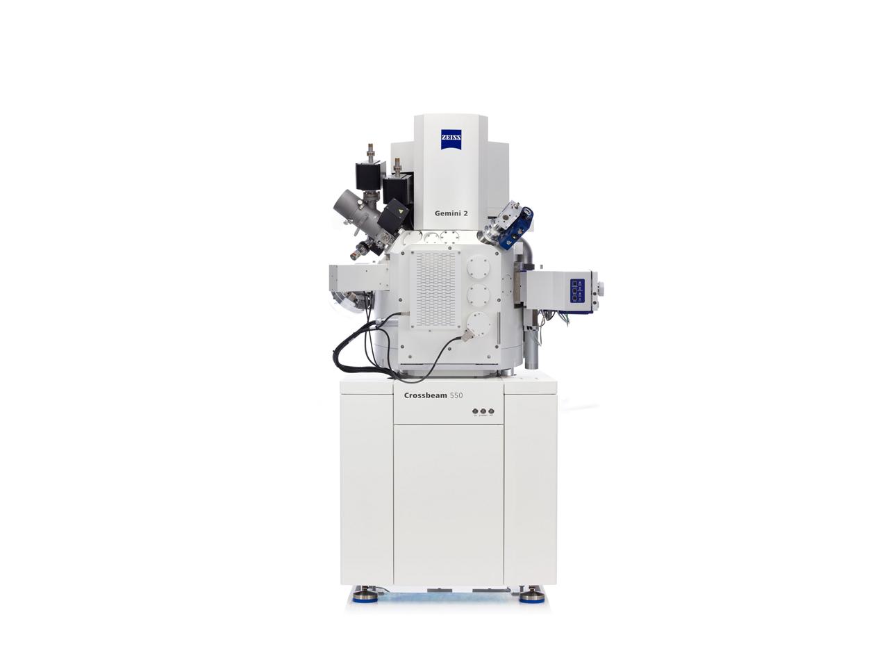
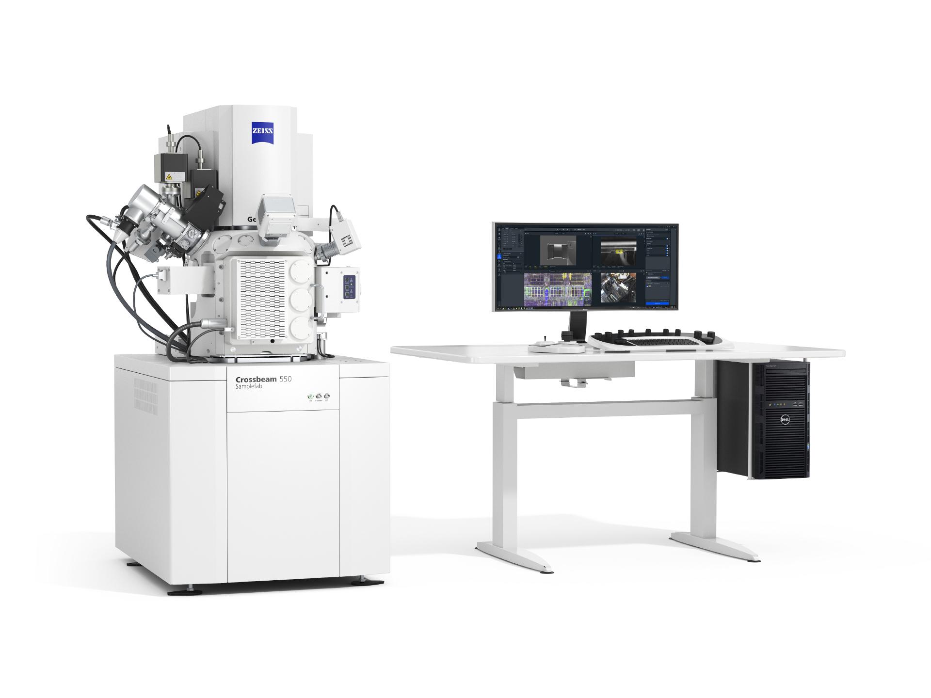
Explore ZEISS GeminiSEM FE-SEM
Recommended Products for Development and Failure Analysis of Advanced Semiconductor Devices


Semiconductor Lab Essentials


Microscopy FAQs for Semiconductors
ZEISS offers a variety of microscopy techniques tailored for Semiconductors including:-
Zeiss microscopes, especially the Crossbeam FIB-SEMs, enhance the yield and success of Transmission Electron Microscopy (TEM) lamellae preparation for semiconductor failure analysis through several key features:
- High-Resolution Imaging: Essential for Identifying Target Areas and Assessing Sample Quality.
- FIB (Focused Ion Beam) Milling: Ga+ focused ion beam – scanning electron microscope (FIB-SEM) for preparing TEM samples with minimal artifacts through simultaneous Imaging while milling and precise end-pointing.
- Integrated Analytics: Provides additional insights, such as EDS Elemental Analysis, and Real-Time Feedback during milling to allow quick adjustments and quality enhancement of the lamella.
- Automation: Supports semi-automated and automated TEM lamellae prep workflows, optimizing efficiency, yield and success rates.
-
Electron microscope-based techniques like Passive Voltage Contrast (PVC) and Nanoprobing are crucial for defect localization and electrical fault isolation in semiconductor devices.
- Passive Voltage Contrast (PVC): Uses SEM to visualize electrical potential differences within semiconductor nanostructures, aiding in defect and fault identification.
- Nanoprobing: Utilizes sharp probes for precise electrical measurements on specific nanoscale features that can only be observed under an SEM. Key nanoprobing modes include:
- Electron Beam Absorbed Current (EBAC): Measures current from electron absorption, revealing local electrical properties and tracing carrier path.
- Electron Beam Induced Current (EBIC): Detects current from electron beam interaction, mapping p-n junctions and electrically active defects.
- Electron Beam Induced Resistance Change (EBIRCH): Identifies resistive defects like shorts.
Zeiss GeminiSEM field-emission SEMs allow for seamless integration of imaging and nanoprobing, enabling real-time observation of the electrical characteristics of the device while simultaneously visualizing its structure.
Explore ZEISS GeminiSEM FE-SEM
To learn more about electrical defect localization inside an SEM and Passive Voltage Contrast, please listen to our recent webinar. -
Nanoscale tomography provides high-resolution, three-dimensional imaging of semiconductor structures, allowing for detailed visualization of internal features and defects. This technique enables precise identification and localization of faults, such as voids, inclusions, and interface irregularities, which are critical for understanding failure mechanisms and improving device reliability.
By reconstructing the 3D architecture of semiconductor devices, nanoscale tomography in a focused ion beam scanning electron microscope (FIB-SEM) facilitates a comprehensive analysis of complex structures, aiding in the development and optimization of advanced semiconductor technologies. True z-depth monitoring with high nm-scale resolution, live imaging while milling, isotropic voxels and integrated analytics are few key features to obtain most accurate 3D reconstruction of the complex structure.