advanced microscopy techniques

New Frontiers in Nanomaterials

Unlock the Secrets of Nanoscale Materials with Precision and Clarity
Empowering Nanomaterials Research​ With the rapid advancements in microscopy techniques, you now have access to an array of innovative tools designed to enhance nanoscale visualization and overcome previous limitations. Whether you're grappling with complex structures or seeking finer details, cutting-edge imaging technologies are paving the way for clearer insights and groundbreaking discoveries. Embrace these advancements with confidence, knowing that the path to unlocking the mysteries of the nanoscale is filled with opportunities for exploration and innovation. Your dedication to pushing the boundaries of knowledge is supported by a wealth of resources and techniques that can elevate your research to new heights.
  • Unparalleled Imaging​

    Image and characterize almost any material with nanometer resolution and enhanced signal.​

  • High Precision Nanofabrication​

    ​Prepare nanostructured devices with the stability, automation, and ease-of-use for your nanopatterned structures.

  • Effortless Sample Preparation​

    ​Prepare samples for TEM or APT analysis using powerful automation and end-point control.

Drive Innovation with Exceptional Nanoscale Results​

See the tools and methods used for breakthroughs in nanostructured materials

Fundamental Material Physics

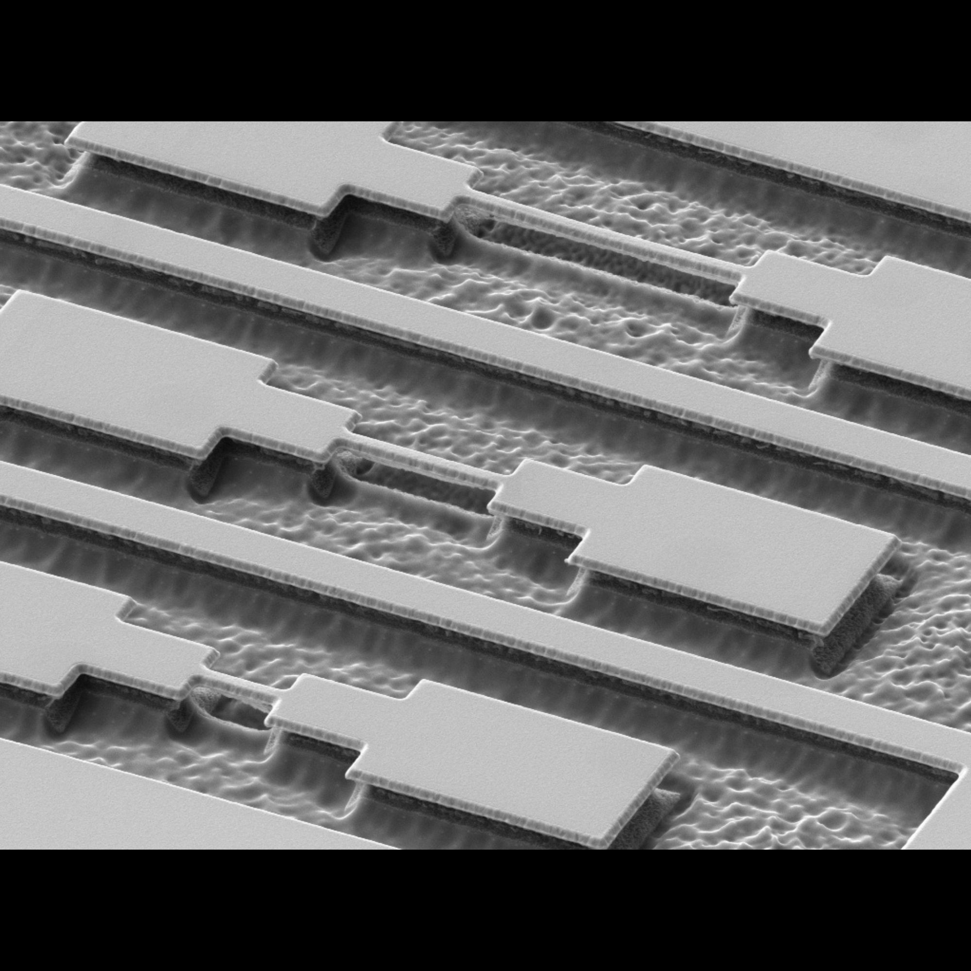
Create precise nanometer-scale objects easily and reliably using in-column deceleration combined with electromagnetic and electrostatic lens technology for material innovations in fields such as photonics, optoelectronics, plasmonics, and quantum technology.

Image Delicate Materials

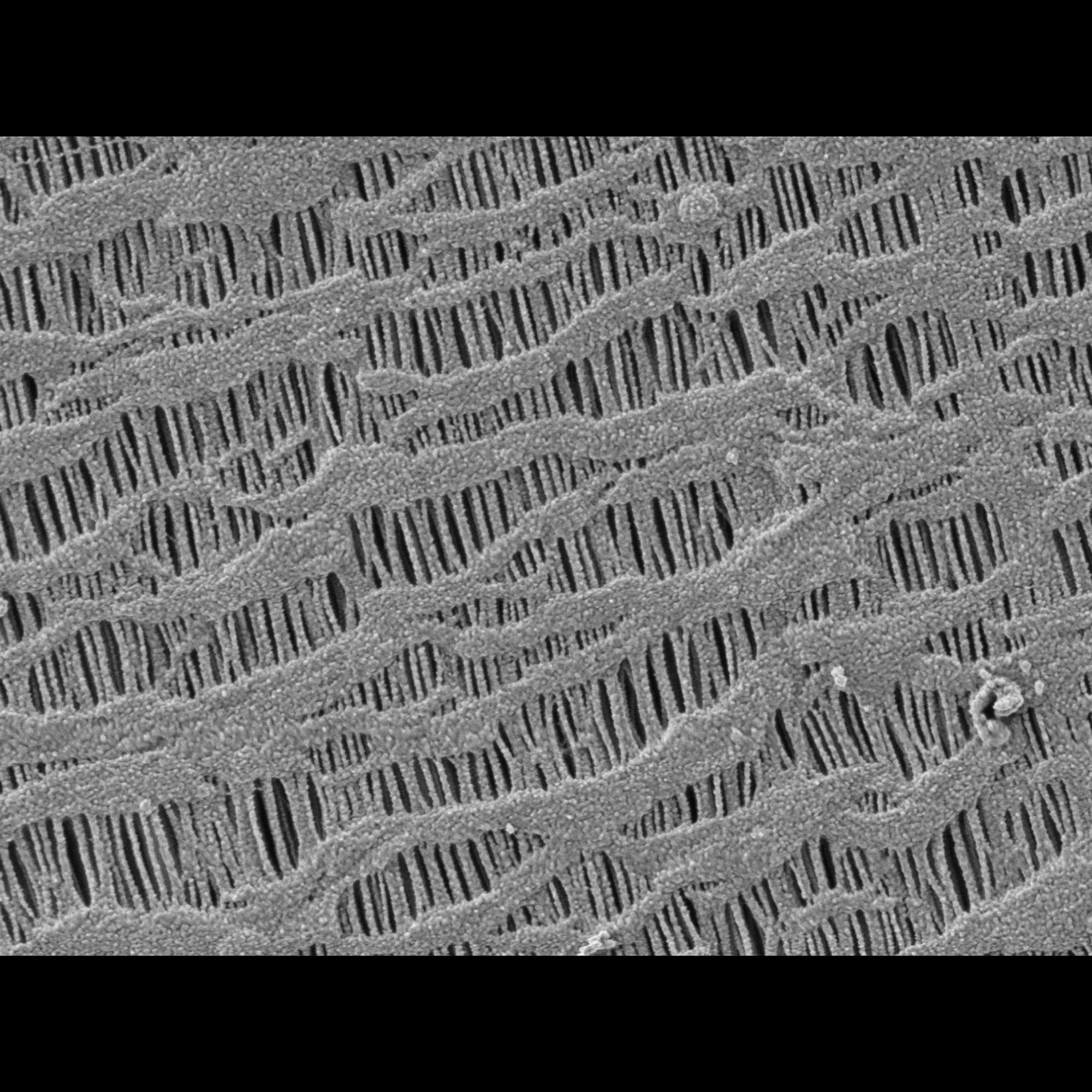
Image your samples in their native state without sacrificing image quality or resolution. Utilize the power of in-column beam deceleration and C-DIC technology to image the most beam-sensitive materials.

Prototyping Next-Gen Nanostructures

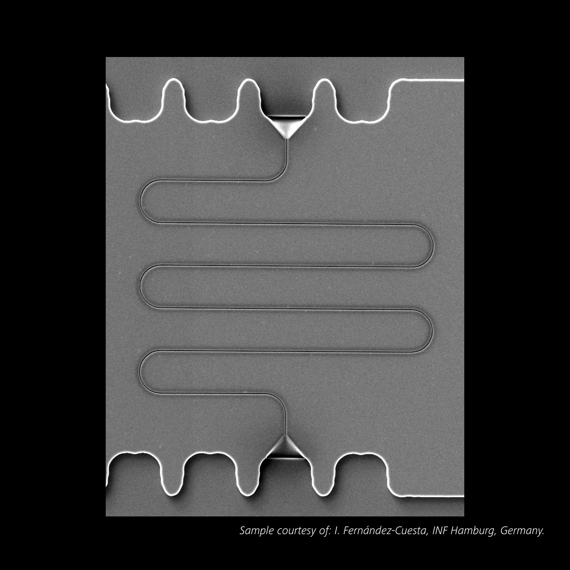
Gain the precision and advanced patterning capabilities needed for prototyping advanced devices for innovations in areas such as medicine, communications, and more.

Investigating Thin Film Properties

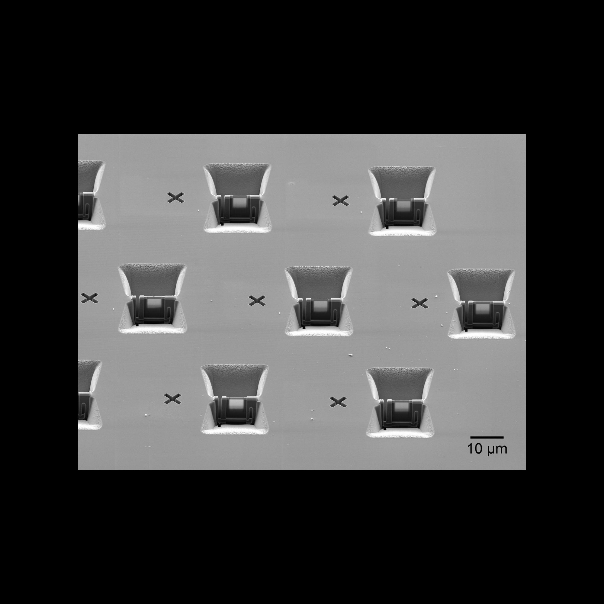
Prepare samples for further investigation in TEM with powerful automation and unparalleled precision and efficiency.

Studying Micromechanics

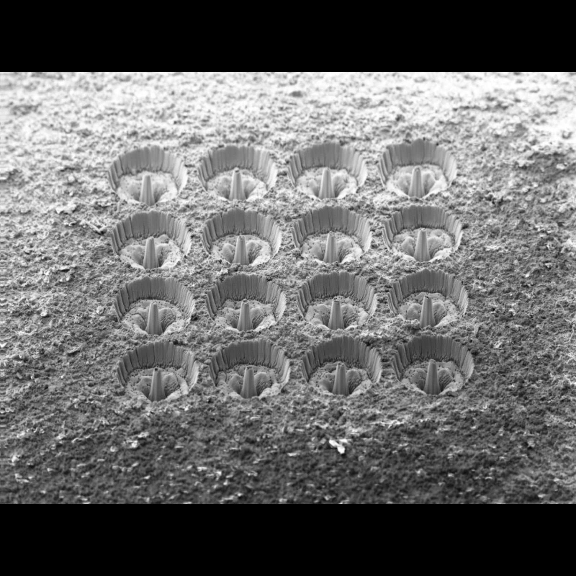
Prepare samples with ease, precision and speed for micromechanical testing with automated fs-laser milling.

Aging Studies in SOECs

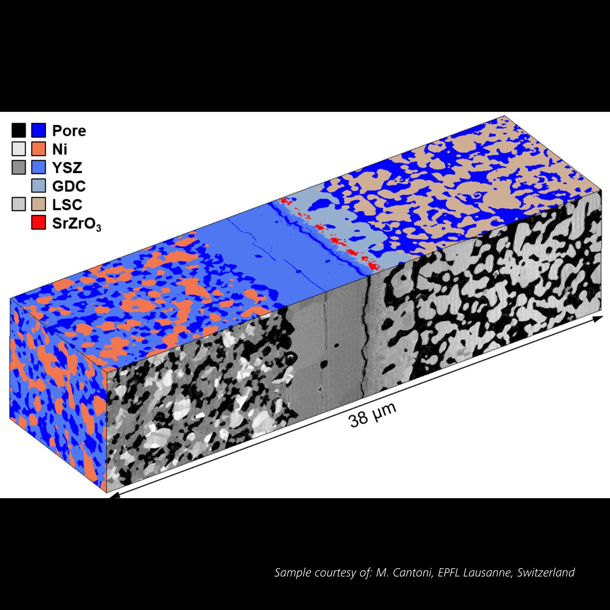
Gain deeper insights into the resistance of solid oxide electrolysis cells (SOEC) to thermal cycling and their improved lifetime through high-resolution 3D analysis.

What You Can Do

  • <10 nm

    Patterning capability with the ZEISS Crossbeam

  • Full 200 mm​

    Sample size capability without the need to rotate your sample on ZEISS Crossbeam and Gemini SEMs​

  • >60 hours​

    Constant FIB beam current for long milling operations on the ZEISS Crossbeam ​

  • 4nm​

    Isotropic voxels with Atlas 5 for the highest resolution 3D FIB tomography​

  • 33 mins​

    to prepare a pillar for APT or for micromechanical testing with ZEISS Laser FIB​

Complete your lab

with our new solution bundles

You can enhance your Nanoscience & Functional Materials Research with the following solutions

What types of microscopy techniques are available for nanomaterials research at ZEISS?

ZEISS offers a broad spectrum of microscopy techniques for nanomaterials research, including:
  • ZEISS offers a variety of microscopy techniques for nanoscience research, including:​
    • Field Emission SEM: Characterization is fundamental to materials science research, making ultra-high resolution electron microscopy crucial for understanding the structure and morphology that determine material properties.​
    • Focused Ion Beam SEM: Whether you're fabricating nanodevices to study superconducting nanowires or preparing TEM lamella for thin film analysis of CIGS and perovskite materials for next-generation solar cells, a FIB-SEM is essential for manipulating and fabricating materials at the nanometer scale.​
    • Advanced Patterning Software: Enhances your process with simultaneous beam control for both ion and electron beams, smart operation recipes for consistent milling and deposition, optimized experiment design using 3D profiles and array builder tools and save up to 40% milling time with Fastmill for efficient FIB cross-section preparation.​
    • ZEN Core EM: Standardize imaging workflows on ZEISS microscopes, from SEMs and FIB-SEMs to light microscopes, with an intuitive, consistent, and customizable user interfaces that allow you to focus on your science rather than being a microscopist.​
    These techniques form a solid foundation for nanoscience research and will deliver the results you need to keep your research moving forward.
  • ZEISS microscopy solutions enable nanomaterials research by offering:​

    • Sample Versatility: ZEISS microscopy solutions offer a broad spectrum of light, electron, and FIB microscopes, providing flexibility to analyze diverse nanomaterials and structures with precision and adaptability.​
    • High-Precision Sample Preparation: The ZEISS Crossbeam dual FIB enables meticulous sample preparation for TEM lamella and nanomachining, ensuring high-quality results for detailed nanofabrication research.​
    • AI-based Image Analysis: ZEISS software utilizes AI-based models to streamline complex image analyses, facilitating automated segmentation, feature extraction, and quantitative measurements for insightful data interpretation.​
    • Connected Imaging: Seamless integration of imaging data from light, electron, and FIB microscopy, along with third-party datasets, provides comprehensive characterization of nanomaterials at multiple scales, enhancing the depth and breadth of nanoscience research.​

          Together, these solutions enable you to unlock new insights and push the boundaries of neuroscience research.

        • ZEISS technology is used everyday to advance research in nanomaterials and nanofabricated devcies. Here are a few examples:​

          • ​Fabrication of Nanofluidic Devices: Direct FIB nanopatterning on silicon master stamps facilitates quick prototyping of nanochannels in diverse shapes, cross-sections, and depths. ​
            ZEISS Solutions for Micro- and Nanofluidics​
          • ​CIGS Solar Cells: FIB cross sections of SIGS solar cells on different substrates reveal the internal structure of the cell and for subsequent analysis using STEM, EDS, and SIMS.​
            Inspired by our customer stories?​
          • Microstructural Analysis of Battery Cathodes: Machine learning-based segmentation methods provide a more accurate segmentation results as compared to classic thresholding.​
            Quantitative Microstructural Analysis of State-of-the-art Lithium-ion Battery Cathodes​

              These are just a few examples—explore our website to discover more resources tailored to your nanomaterials research needs.

            Discover Our Application Hub

            Comprehensive solutions and capabilities

            Explore applications and discover tailored solutions for you industry needs.