Advanced Microscopy Techniques
Precision Unlocked for Semiconductors
Discover flawless detail at every step
Scroll animation items

Advanced Packaging and 3D Heterogeneous Integration
ZEISS solutions achieve significant advancements for package failure analysis workflows. By providing superior imaging and cross-sectional analysis, as well as a correlated workflow using artificial intelligence (AI), ZEISS delivers new insights from macroscale to nanoscale with fast time to results.

Semiconductor Device Development and Failure Analysis
Semiconductor products serve the needs of transportation, work, social communication, and industrial infrastructure. There is constant demand for higher computing performance in ever smaller form factors. Logic and memory semiconductor structure analysis is challenged by novel materials and increasingly complex geometries. Shrinking transistor sizes at the newest technology nodes demand the highest performance for electron microscopy and nanoprobing applications.


Advanced Analysis for Complex New Materials and Structures
The mobile communication, Internet of Things (IoT), cloud computing, and the electrification of automotive industries are driving huge demand for high-performing “More than Moore” semiconductor devices, which require the integration of new materials and processes, or novel silicon architectures and packaging technologies such as micro-electromechanical systems (MEMS). Direct band gap and wide band gap materials such as gallium arsenide (GaAs), silicon carbide (SiC), and gallium nitride (GaN) present new challenges to equipment manufacturers and device fabricators alike. Many of these devices also integrate traditional ICs, which creates fabrication and packaging challenges.

Improved Production Yields of Defect-Free Devices
Consumer demand for brighter and more interactive display panels in electronic products is driving innovation in the highly competitive display industry. Display technology is evolving, with LCD and rigid organic light-emitting-diode (OLED) technology now produced in large volumes at low cost, and premium consumer products offering flexible OLED and microLED displays.
OLED, microLED and photonics applications are complex systems utilizing sensitive and difficult-to-analyze materials that demand advanced microscopy technologies in their development and manufacture.


Recommended Products for Semiconductor & Electronics Research
Buy Online, Get a Quote or Trial


Video Library
Text that elaborates on the main headline above


FAQs for ZEISS in Neuroscience
-
Yes, ZEISS provides various case studies and application notes that showcase the use of their microscopy systems in neuroscience. Examples include:
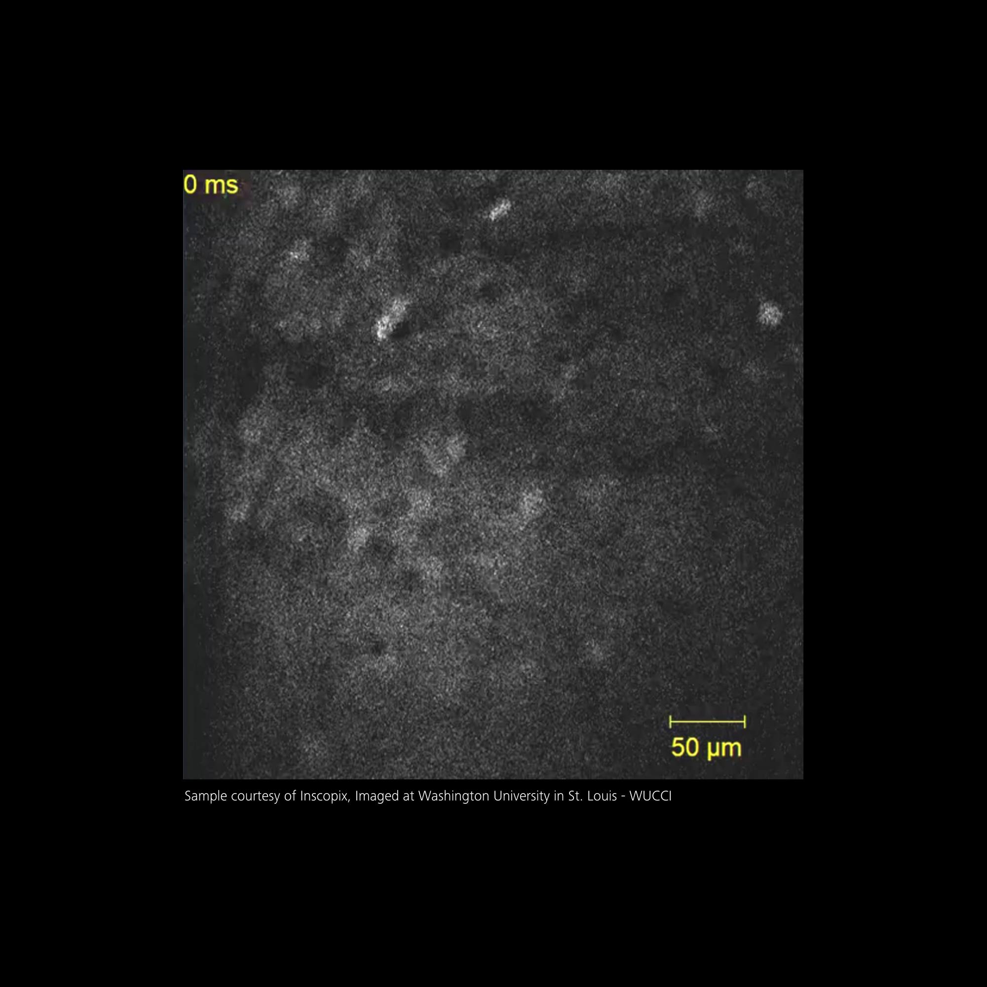
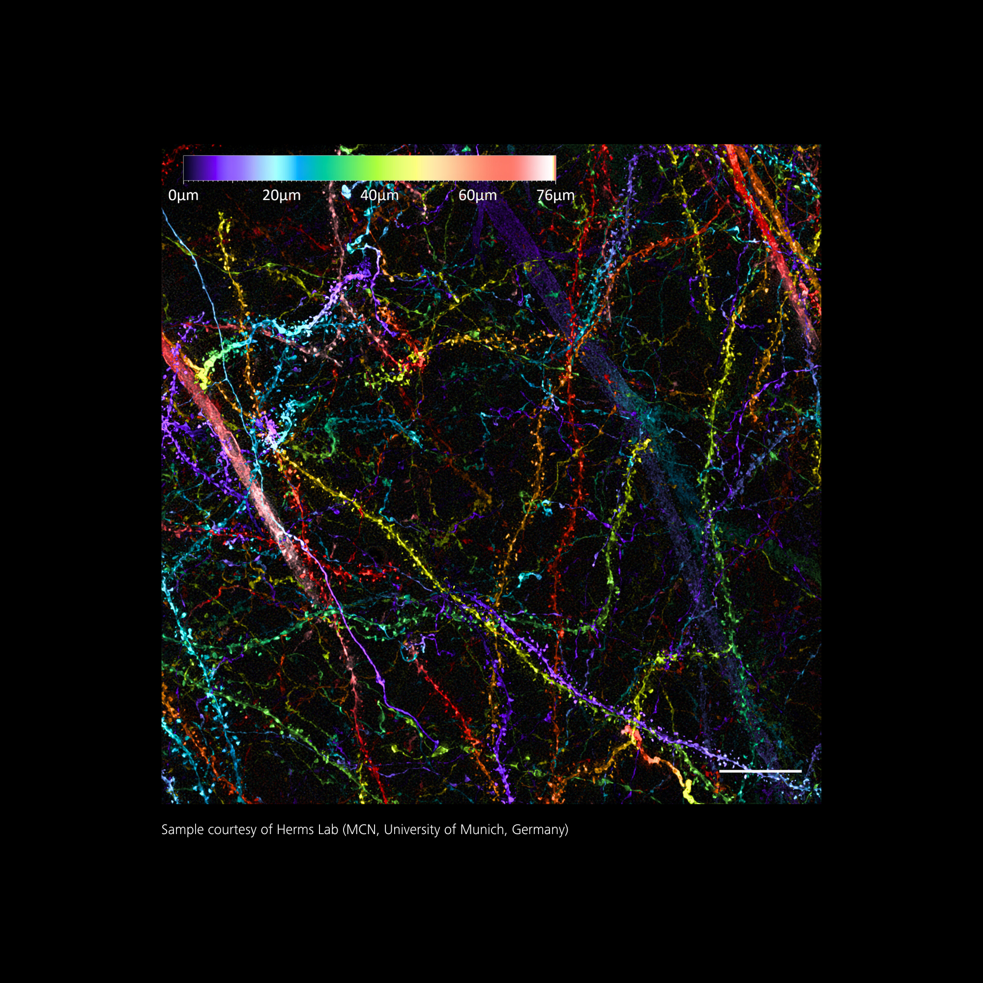
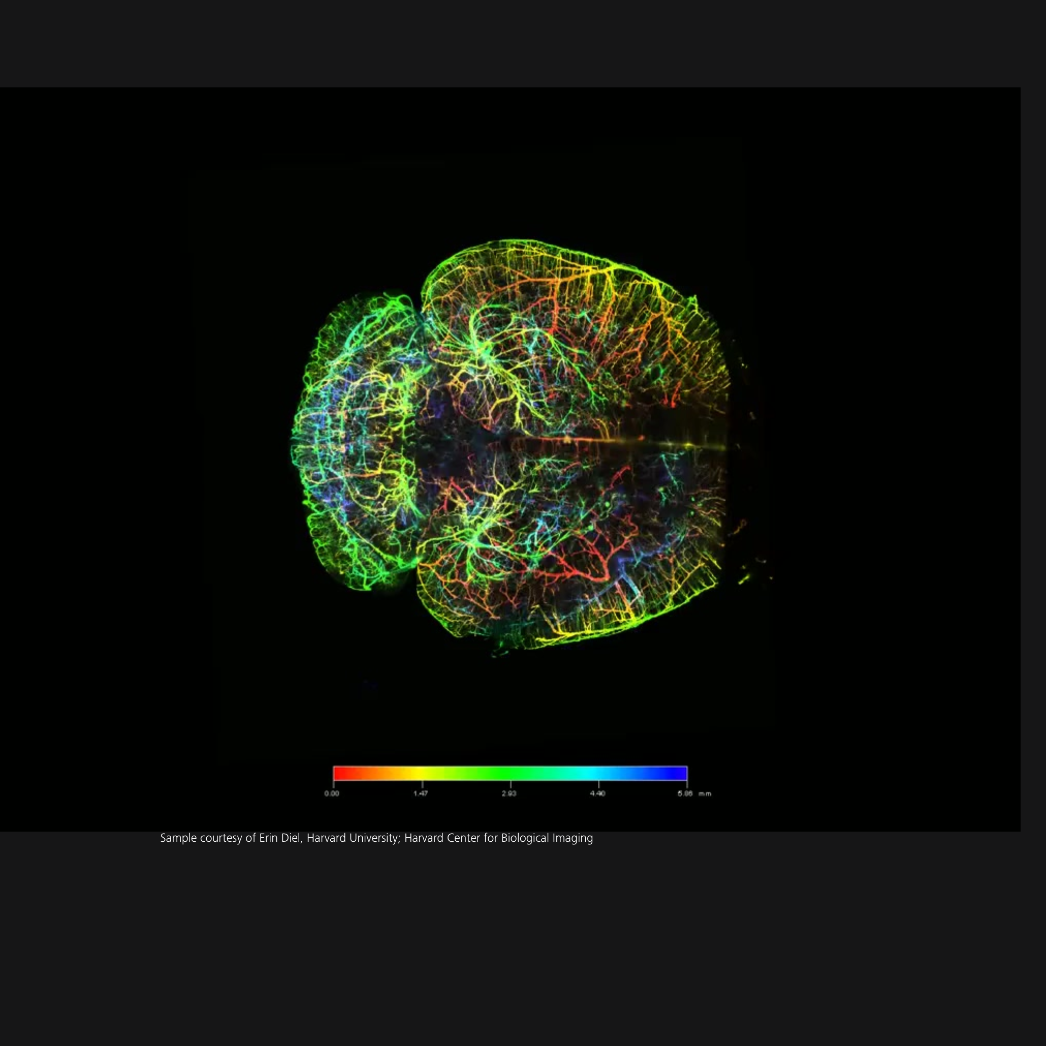
- Imaging Synaptic Structures: Using confocal microscopy to study synaptic connections and plasticity.
- Neurodegenerative Disease Research: Employing two-photon microscopy to observe changes in neuronal behavior in live animal models.
- Brain Mapping: Utilizing advanced imaging techniques to visualize brain connectivity and function.
-
ZEISS microscopy solutions enhance neuroscience research by providing:
- High Resolution: Advanced optics and imaging technologies allow for detailed visualization of neuronal structures and processes.
- Live Imaging: Many systems are designed for live-cell imaging, enabling the observation of dynamic processes in real-time.
- Multimodal Imaging: The ability to combine different imaging modalities (e.g., fluorescence and electron microscopy) allows for comprehensive analysis of samples.
These features facilitate a deeper understanding of neural mechanisms and contribute to advancements in neuroscience.
-
ZEISS offers a variety of microscopy techniques tailored for neuroscience research, including:
- Confocal Microscopy: Ideal for imaging thick samples and obtaining high-resolution images of cellular structures.
- Two-Photon Microscopy: Particularly useful for imaging living tissues at greater depths, minimizing photodamage.
- Electron Microscopy: Provides ultra-high resolution for detailed visualization of neuronal structures.
These techniques enable researchers to explore complex neural networks and cellular interactions in detail.