
Introduction to TEM Lamella Preparation On Your ZEISS FIB-SEM
A ZMCC SkillBuilder Workshop
Workshop Overview & Agenda
This workshop is an introduction to Transmission Emission Microscopy (TEM) lamella preparation using SmartSEM and SmartFIB on a ZEISS FIB-SEM tool. A basic understanding of scanning electron microscopy (SEM), basic experience with SmartSEM and SmartFIB software and with Ga+ focused ion beam (FIB) milling are required. No prior experience with TEM lamella preparation is required.
This is a 3-hour workshop during which attendees will be shown the workflow for preparing a TEM lamella using the ZEISS Crossbeam 550 tool with an Oxford OmniProbe 400. This includes milling parameter selection, tips for efficient workflow execution, methods for maximizing specimen quality and live monitoring of the thickness of the lamella for endpointing.
It is recommended that attendees secure time on their own instruments after the workshop session to practice what was shown using their own samples.
Who should attend?
- FIB-SEM owners that want to understand how to prepare their own TEM lamella.
- Infrequent FIB-SEM users in need of a refresher on TEM lamella preparation.
- Lab managers, engineers or technicians looking to improve the quality of TEM lamella they prepare.
Learning objectives after completion of this workshop, attendees should:
- Improved understanding of the steps required to prepare a TEM lamella on a ZEISS FIB-SEM tool.
- Improved parameter selection and methods for optimizing the quality of the TEM lamella.
- Efficient execution of the TEM lamella preparation workflow.
This is a paid workshop.
Spots are limited.
Access to a SEM after each day is strongly recommended to apply lessons learned and share results with applications team for further support.
Preview the topics covered below and register for the workshop here.
Topics
- Introduction and basics of TEM lamella preparation on a FIB-SEM tool with Ga+ FIB.
- Setting up the FIB-SEM on a ZEISS Crossbeam 550
- Brief review of SmartSEM and SmartFIB for imaging and patterning, including milling recipe / pattern selection.
- Automated bulk lamella preparation
- Preparation of a TEM lamella from bulk to final thinning.
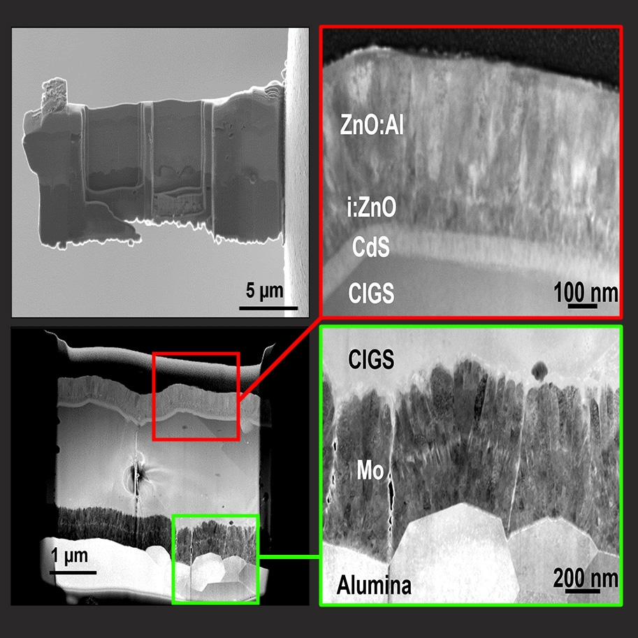
- Examples of SEM and STEM images of TEM lamellae imaged on a ZEISS GeminiSEM microscope
Session
After the workshop sessions, the attendees are strongly encouraged to attempt the methods shown on their own systems with their own samples. Screen sharing sessions to review the data can be setup with the applications team through independent email threads. Our support team will assist in further optimization and answer any questions to help attendees acquire the best data possible.

Michael has been working with and promoting FIB-SEM microscopy solutions for over 20 years. He has been an Applications Engineer with ZEISS since 2021 working primarily with GeminiSEMs and Crossbeams. Michael has a background in physics centered around materials science and has extensive experience collaborating with scientists and engineers within the areas of microelectronics materials and process characterization as well as physical failure analysis of microelectronics.
Register for the workshop
This workshop costs $400 per attendee. Please fill out the form below to initiate your registration, and be sure to submit your payment at the link in the automated follow-up email to finalize your registration.
To secure your seat, please submit your payment by May 22, 2024.