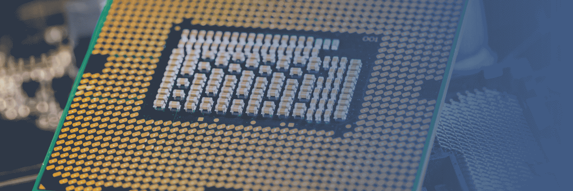

Semiconductor Advanced Packaging and 3D Heterogeneous Integration
Improve Productivity with Multi-dimensional Correlative Imaging & Analysis
Non-destructive 3D Tomography of Heterogeneous Integration Package
Buried defects in interconnect bridge connecting multiple chips can be costly and detrimental to the performance. 3D X-ray imaging and analysis helps in accelerating the failure analysis

3D X-ray Image of Heterogeneous Package


3D Reconstructed Image
75 µm C4 bumps and 30 µm microbumps


Virtual Cross Section of Microbumps


Virtual Cross Section of Microbumps
30 µm microbumps imaged at 0.8 µm/voxel resolution


Virtual Cross Section of C4 Bumps


Virtual Cross Section of C4 Bumps
75 μm C4 bumps imaged at 0.8 μm/voxel resolution


3D Package Interconnects
Rapid Access and Analysis of Deeply Buried Interconnects
Reducing total time to results to less than an hour for accessing deeply buried features can accelerate failure analysis as well as potentially mitigate costly process deviations.
Left: 3D IC prepared using laser ablation and FIB polishing in Crossbeam-Laser.
Right: Backscattered electron image of microbump.
Explore ZEISS Crossbeam-Laser


Large FOV of 2.5D Package Interconnects
High-resolution, Extreme Field of View Imaging
Improve productivity and efficiency of package and BEOL structures with distortion-free, large field of view provided by GeminiSEM.
Inset: Close up of 2.5D package cross section shows grain structure and solder crack in 20 µm microbump.


Intermetallic Layers in Solder Bumps
Intermetallic Layer Analysis of Solder Bumps
Identify interfacial failure with cross-section of a flip-chip solder bump utilizing superior material contrast and channeling contrast of grain structure.
Inset: Failure at the UBM RDL interface.
Recommended Products for Multi-dimensional Imaging and Analysis of Semiconductor Packages


Semiconductor Lab Essentials


Microscopy FAQs for Semiconductors
ZEISS offers a variety of microscopy techniques tailored for Semiconductors including:-
Imaging and identification of buried features and defects in 3DHI packages are challenging because of complex multi-layer nano- and micro-structures, sub-micron length scale of defects, heterogeneous materials and the requirement of nondestructive defect localization.ZEISS X-ray microCT and 3D X-ray microscopes provide the necessary tools and capabilities to overcome the challenges of imaging and identifying buried features and defects in heterogeneous integration packages. Key benefits include sub-micron resolution nondestructive imaging, advanced phase and absorption contrast detection, access and imaging stability for samples of different shapes and sizes, AI-assisted fast high-resolution 3D reconstruction and segmentation.
-
Accessing and analyzing any buried feature and/or defect in a semiconductor package is time consuming and challenging. To access the nano- and micro-scale features inside the chip, delicate but fast milling techniques are necessary.
By combining femto-second laser ablation, FIB-milling, high-resolution imaging and analytics, the Zeiss Crossbeam Laser system facilitates quick access and thorough analysis of buried defects in semiconductor packages, enhancing efficiency and accuracy in defect characterization and failure analysis.
-
Nanoscale tomography provides high-resolution, three-dimensional imaging of semiconductor structures, allowing for detailed visualization of internal features and defects. This technique enables precise identification and localization of faults, such as voids, inclusions, and interface irregularities, which are critical for understanding failure mechanisms and improving device reliability.
By reconstructing the 3D architecture of semiconductor devices, nanoscale tomography in a focused ion beam scanning electron microscope (FIB-SEM) facilitates a comprehensive analysis of complex structures, aiding in the development and optimization of advanced semiconductor technologies. True z-depth monitoring with high nm-scale resolution, live imaging while milling, isotropic voxels and integrated analytics are few key features to obtain most accurate 3D reconstruction of the complex structure.


