

Accelerate Development of Displays, LEDs and Photonic Devices
By accurate microstructural imaging and fault isolation
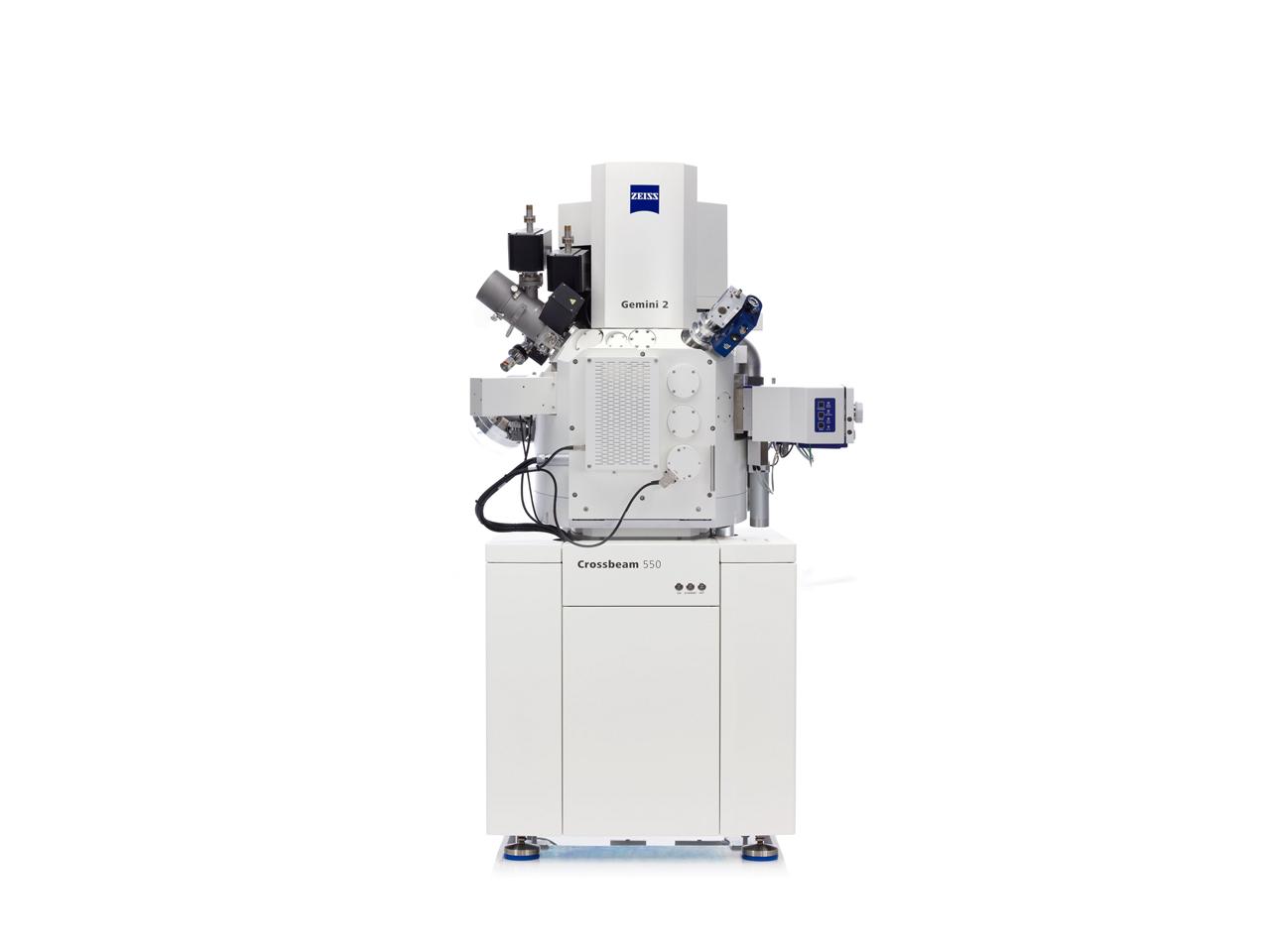
Failure Analysis of Image Sensor
Spatial cracks and other sub-surface defects are challenging to identify without nanoscale 3D tomography. ZEISS Crossbeam accelerates the fault isolation and failure analysis using nm-scale FIB-tomography with isotropic voxels and precise depth monitoring.
The video shows 3D FIB-SEM tomography dataset of an image sensor, with (15 nm)3 voxel size.
Defect Inspection of Entire Camera Modules
Nondestructive 3D defect inspection for camera modules (e.g., in smartphones) is crucial for process monitoring and failure analysis. ZEISS 3D X-ray imaging technology enables faster turnaround time using unique resolution-at-a-distance (RaaD), various phase and absorption contrast detection and AI-assisted 3D reconstruction and image segmentation.

3D Reconstruction of Smartphone Camera Module
3D Reconstruction of Smartphone Camera Module
Camera module acquired at 18 µm/voxel resolution shows CMOS imaging sensor and other mechanical components.


Smartphone Camera Lens Analysis
Smartphone Camera Lens Analysis
Virtual cross section focusing on six-layer optical lens stacks imaged at 18 µm/voxel resolution.
Recommended Products for Multi-dimensional Imaging and Analysis of Semiconductor Packages


Semiconductor Lab Essentials


Microscopy FAQs for Semiconductors
ZEISS offers a variety of microscopy techniques tailored for Semiconductors including:-
ZEISS microscopes, especially the Crossbeam FIB-SEMs, enhance the yield and success of Transmission Electron Microscopy (TEM) lamellae preparation for semiconductor failure analysis through several key features:
High-Resolution Imaging: Essential for Identifying Target Areas and Assessing Sample Quality.
FIB (Focused Ion Beam) Milling: Ga+ focused ion beam – scanning electron microscope (FIB-SEM) for preparing TEM samples with minimal artifacts through simultaneous Imaging while milling and precise end-pointing.
Integrated Analytics: Provides additional insights, such as EDS Elemental Analysis, and Real-Time Feedback during milling to allow quick adjustments and quality enhancement of the lamella.
Automation: Supports semi-automated and automated TEM lamellae prep workflows, optimizing efficiency, yield and success rates.
-
Nanoscale tomography provides high-resolution, three-dimensional imaging of semiconductor structures, allowing for detailed visualization of internal features and defects. This technique enables precise identification and localization of faults, such as voids, inclusions, and interface irregularities, which are critical for understanding failure mechanisms and improving device reliability.
By reconstructing the 3D architecture of semiconductor devices, nanoscale tomography in a focused ion beam scanning electron microscope (FIB-SEM) facilitates a comprehensive analysis of complex structures, aiding in the development and optimization of advanced semiconductor technologies. True z-depth monitoring with high nm-scale resolution, live imaging while milling, isotropic voxels and integrated analytics are few key features to obtain most accurate 3D reconstruction of the complex structure.
-
Accessing and analyzing any buried feature and/or defect in a semiconductor package is time consuming and challenging. To access the nano- and micro-scale features inside the chip, delicate but fast milling techniques are necessary.
By combining femto-second laser ablation, FIB-milling, high-resolution imaging and analytics, the Zeiss Crossbeam Laser system facilitates quick access and thorough analysis of buried defects in semiconductor packages, enhancing efficiency and accuracy in defect characterization and failure analysis.

