Press Release

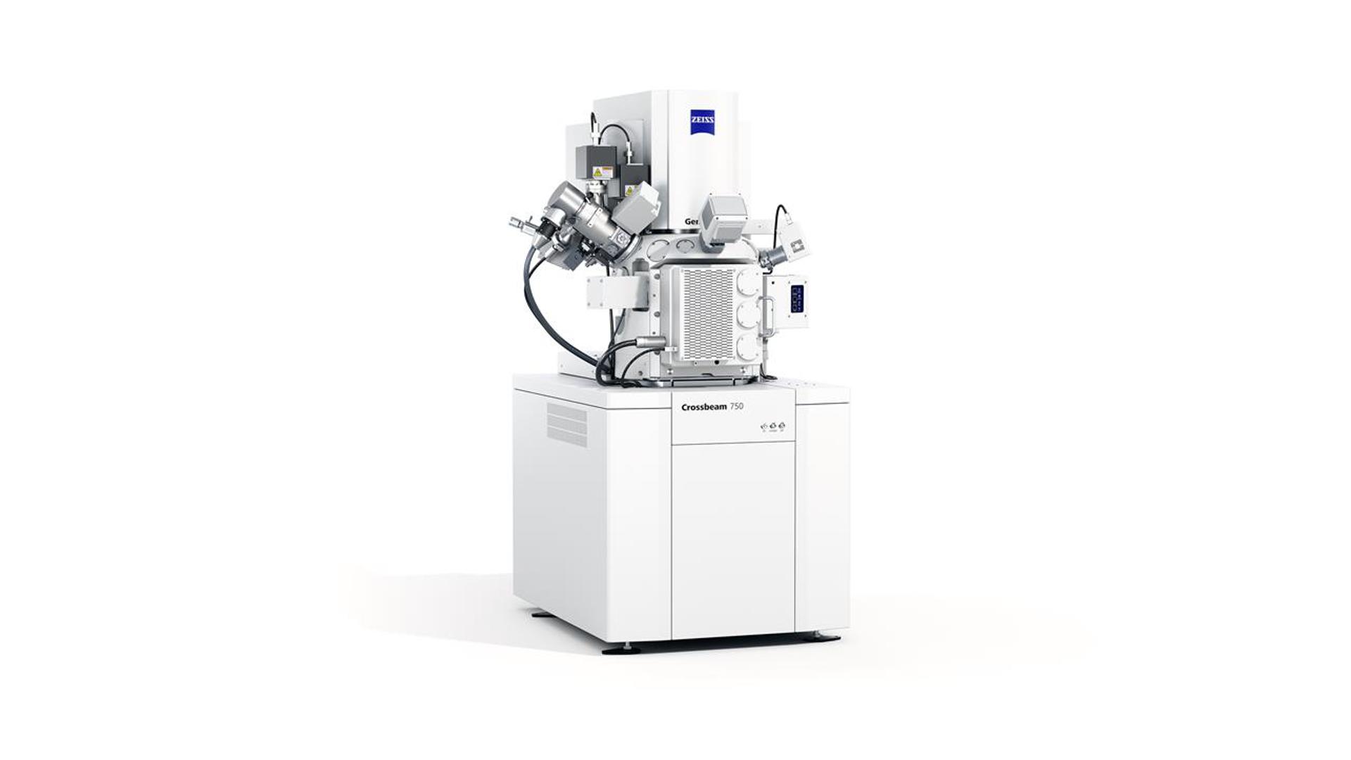
New ZEISS Crossbeam 750 FIB-SEM for high-accuracy sample preparation workflows

Advances in simultaneous SEM imaging while FIB milling provide unmatched feedback for precision endpointing
31 March 2026
  • New ZEISS Gemini 4 electron optics offer superior resolution and signal-to-noise ratio
  • Live SEM imaging extended to monitor rapid FIB milling down to ultrafine lamella polishing
  • Largest undistorted field-of-view supports the best outcomes in 3D tomography and APT workflows
Jena, Germany | 31 March 2026 | ZEISS Research Microscopy Solutions

ZEISS today unveiled the new ZEISS Crossbeam 750 focused ion beam-scanning electron microscope (FIB-SEM) that is optimized for demanding sample preparation. It provides a live, high-resolution “see while you mill” view at any imaging and milling condition to enable immediate feedback and eliminate milling interruptions for uniform first-pass transmission electron microscopy (TEM) lamellae and precise FIB cross sections.

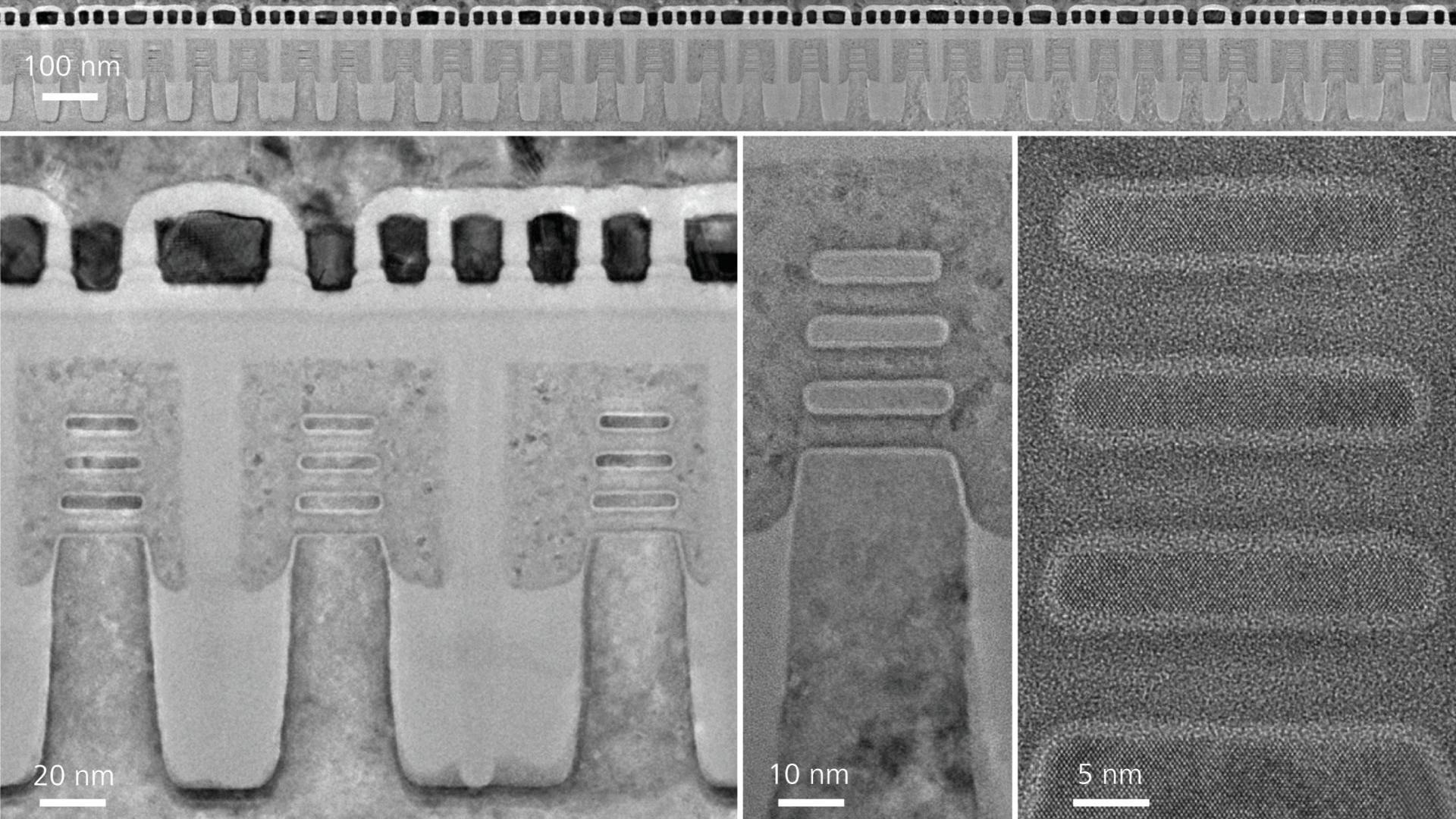
For advanced semiconductor and materials workflows, ZEISS Crossbeam 750 FIB-SEM with new Gemini 4 electron optics delivers background-free, real-time endpointing and sub-nanometer precision for TEM lamellae and high-fidelity three-dimensional (3D) analysis. It is ideal for analysis of leading-node logic and memory devices as well as nanofabrication and 3D volume imaging. For materials research and life sciences, ZEISS Crossbeam 750 speeds acquisition times for 3D tomography through a larger field of view with reduced distortion.

“ZEISS Crossbeam 750 was designed around one core principle: Our customers should not have to stop milling to see where in their sample they are working,” said Dr. Thomas Rodgers, Senior Director of Market Strategy, Head of Business Sector Electronics, ZEISS Microscopy. “Our new high-dynamic-range (HDR) Mill + SEM capability maintains a clear, high-resolution SEM view at any FIB condition, from rapid milling with high FIB currents down to fine polishing at 0.5 kV. This real-time clarity, paired with Gemini 4 electron optics, allows customers to fine-tune processes as they work—reducing rework, improving yield and delivering highly uniform lamellae on the first pass.”

  • 3 nm GAA-FET SRAM TEM images of ZEISS Crossbeam 750 lamella overview.

    3 nm GAA-FET SRAM TEM images of ZEISS Crossbeam 750 lamella (Top) Overview. Gates are perfectly centered over several μm. (Bottom) Higher magnification images of the as-prepared lamella showing preserved crystallinity with minimal amorphization and clearly distinguishable layers.

  • Multi-layered heterostack thin film sample taken with ZEISS Crossbeam 750. Alternating layers of molybdenum disulfide and tungsten disulfide, an advanced novel material subject of research for electronics, photovoltaics, or quantum devices.

    SEM image of a multi-layered heterostack thin film sample taken with ZEISS Crossbeam 750. Alternating layers of molybdenum disulfide and tungsten disulfide, an advanced novel material subject of research for electronics, photovoltaics, or quantum devices. Layers, from top to bottom, are platinum deposition, carbon deposition, heterostack, and silicon dioxide basis. The cross section shows excellent image quality, minimized signal-to-noise ratio, and excellent material contrast.

  • ZEISS Crossbeam 750 FIB-SEM on white background

    ZEISS Crossbeam 750 FIB-SEM advances live, high-resolution “see while you mill” capability, providing unmatched feedback for precision endpointing in sample preparation workflows.

“See while you mill” transforms advanced semiconductor analysis

As semiconductor device architectures shrink and complexity increases—from fin field-effect transistor (finFET) to gate-all-around (GAA), complementary field-effect transistor (CFET), and emerging two-dimensional (2D) materials—precise, real-time control during FIB processing has become critical. ZEISS Crossbeam 750 directly addresses this need by maintaining a clear, high-resolution SEM view during milling, even at low landing energies and at tilt.

The system enables users to observe FIB-sample interactions in real time, fine-tune thinning and polishing steps as they occur, and to hit nanometer-scale endpoints on the first attempt—achieving consistent lamella quality for leading-node logic and memory device and backside power delivery network workflows.

Imaging excellence drives scientific discovery

ZEISS Crossbeam 750 FIB-SEM is essential in materials science workflows for uniform TEM lamella preparation, atom probe tomography (APT) sample prep, nanofabrication (including electron-beam lithography), and high-fidelity 3D volume imaging. For life sciences and materials research, the undistorted large field-of-view of ZEISS Crossbeam 750 and stable low-kV performance improves signal-to-noise and speeds acquisition time.

The ZEISS Crossbeam 750 FIB-SEM is available for ordering now. For more information, please visit www.zeiss.com/crossbeam-750

Press Contact Kristin Unger ZEISS Research Microscopy Solutions

About ZEISS

ZEISS is an internationally leading technology enterprise operating in the fields of optics and optoelectronics. In the previous fiscal year, the ZEISS Group generated annual revenue totaling almost 12 billion euros in its four segments Semiconductor Manufacturing Technology, Industrial Quality & Research, Medical Technology, and Consumer Markets (September 30, 2025).

For its customers, ZEISS develops, produces, and distributes highly innovative solutions for industrial metrology and quality assurance, microscopy solutions for the life sciences and materials research, and medical technology solutions for diagnostics and treatment in ophthalmology and microsurgery. The name ZEISS is also synonymous with the world's leading lithography optics, which are used by the chip industry to manufacture semiconductor components. There is global demand for trendsetting ZEISS brand products such as eyeglass lenses, camera lenses, and binoculars.

With a portfolio aligned with future growth areas like digitalization, healthcare, and Smart Production and a strong brand, ZEISS is shaping the future of technology and constantly advancing the world of optics and related fields with its solutions. The company's significant, sustainable investments in research and development lay the foundation for the success and continued expansion of ZEISS' technology and market leadership. ZEISS invests 15 percent of its revenue in research and development – this high level of expenditure has a long tradition at ZEISS and is also an investment in the future.

With over 46,600 employees, ZEISS is active globally in around 50 countries with more than 60 sales and service locations, around 40 research and development facilities, and 30 production facilities worldwide (September 30, 2025). Founded in 1846 in Jena, the company is headquartered in Oberkochen, Germany. The Carl Zeiss Foundation, one of the largest foundations in Germany committed to the promotion of science, is the sole owner of the holding company, Carl Zeiss AG.

Further information at www.zeiss.com


ZEISS Research Microscopy Solutions

ZEISS Research Microscopy Solutions is the leading provider of light, electron, X-ray microscope systems, correlative microscopy and software solutions leveraging AI technologies. The portfolio comprises of products and services for life sciences, materials and industrial research, as well as education and clinical routine applications. The unit is headquartered in Jena. Additional production and development sites are located in Germany, UK, USA, China and Switzerland. ZEISS Research Microscopy Solutions is part of the Industrial Quality & Research segment.

Further information at www.zeiss.com/microscopy

Press photos

  • Crossbeam 750 GAA-FET TEM

    3 nm GAA-FET SRAM TEM images of ZEISS Crossbeam 750 lamella (Top) Overview. Gates are perfectly centered over several μm. (Bottom) Higher magnification images of the as-prepared lamella showing preserved crystallinity with minimal amorphization and clearly distinguishable layers.

    3 MB
  • Crossbeam 750 heterostack materials

    SEM image of a multi-layered heterostack thin film sample taken with ZEISS Crossbeam 750. Alternating layers of molybdenum disulfide and tungsten disulfide, an advanced novel material subject of research for electronics, photovoltaics, or quantum devices. Layers, from top to bottom, are platinum deposition, carbon deposition, heterostack, and silicon dioxide basis. The cross section shows excellent image quality, minimized signal-to-noise ratio, and excellent material contrast.

    4 MB
  • Crossbeam 750 FIB-SEM

    ZEISS Crossbeam 750 FIB-SEM advances live, high-resolution “see while you mill” capability, providing unmatched feedback for precision endpointing in sample preparation workflows.

    325 KB


Share this article