


3D X-ray Microscopy for Semiconductor Applications:
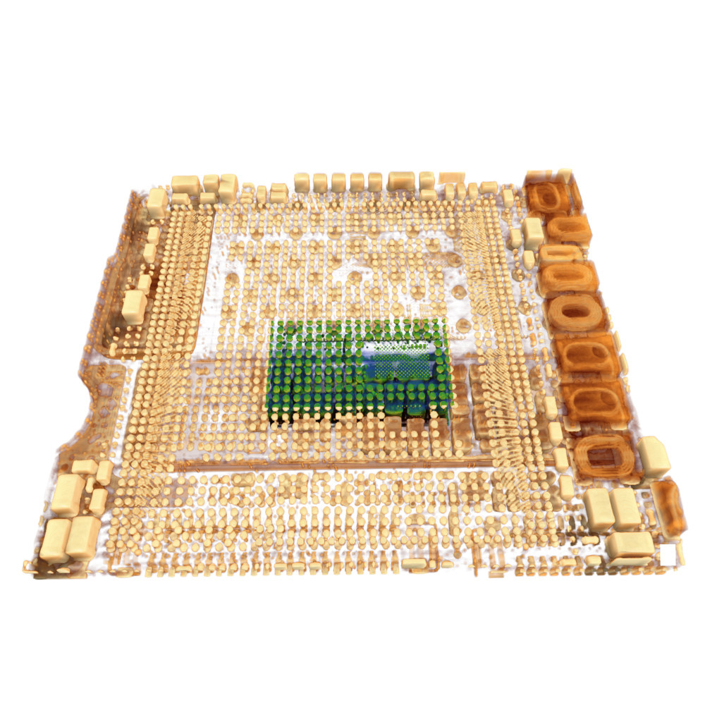
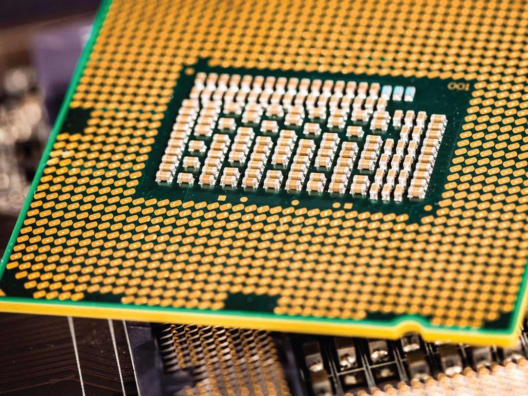
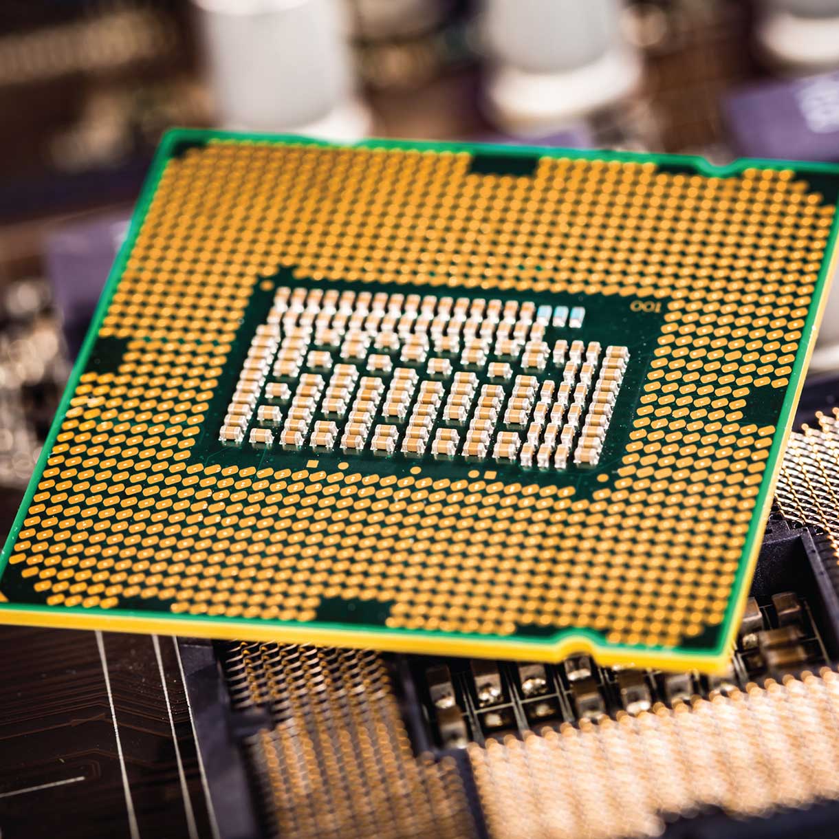
Discover new insights for package failure analysis3D X-ray microscopes (XRM) has been widely adopted in package level failure analysis over the past decade. However, the non-destructive imaging technique is challenged by the emerging architectures, interconnects, and materials in modern IC packages. In this webinar, we will present the recent progress on XRM resolution improvement and data acquisition acceleration through detector optics innovation, AI-based reconstruction implementations, and correlative workflow development. A groundbreaking resolution improvement has been achieved through a detector innovation. Award-winning AI-based reconstruction modules enable 4x faster scans and superior image quality for imaging advanced IC packages. Correlated with laser FIB-SEM microscopy, an XRM to laserFIB workflow has been developed to enable fast and precise failure analysis. For the further demands on resolution and speed in advanced fault isolation, we will report a 50 nm resolution nanotomography technique, recently powered by a deep learning reconstruction method.