
Advanced Defect Localization Techniques in Semiconductor Failure Analysis
Defect localization is a critical step in semiconductor failure analysis, enabling the identification of faults within complex integrated circuits and driving yield improvements in manufacturing processes. In our Defect Localization Webinar Series, we highlight three techniques.
● Session 1: Mastering Semiconductor Defect Localization with Passive Voltage Contrast (available on demand)
● Session 2: Nanoprobing: 10 Signals for Device Characterization & Defect Localization (available on demand)
● Session 3: Conductive AFM: Big Insights from Tiny Places (available on demand)

Mastering Semiconductor Defect Localization with Passive Voltage Contrast
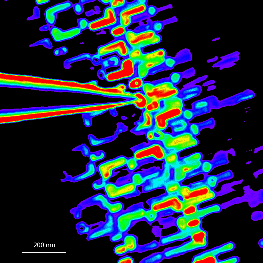
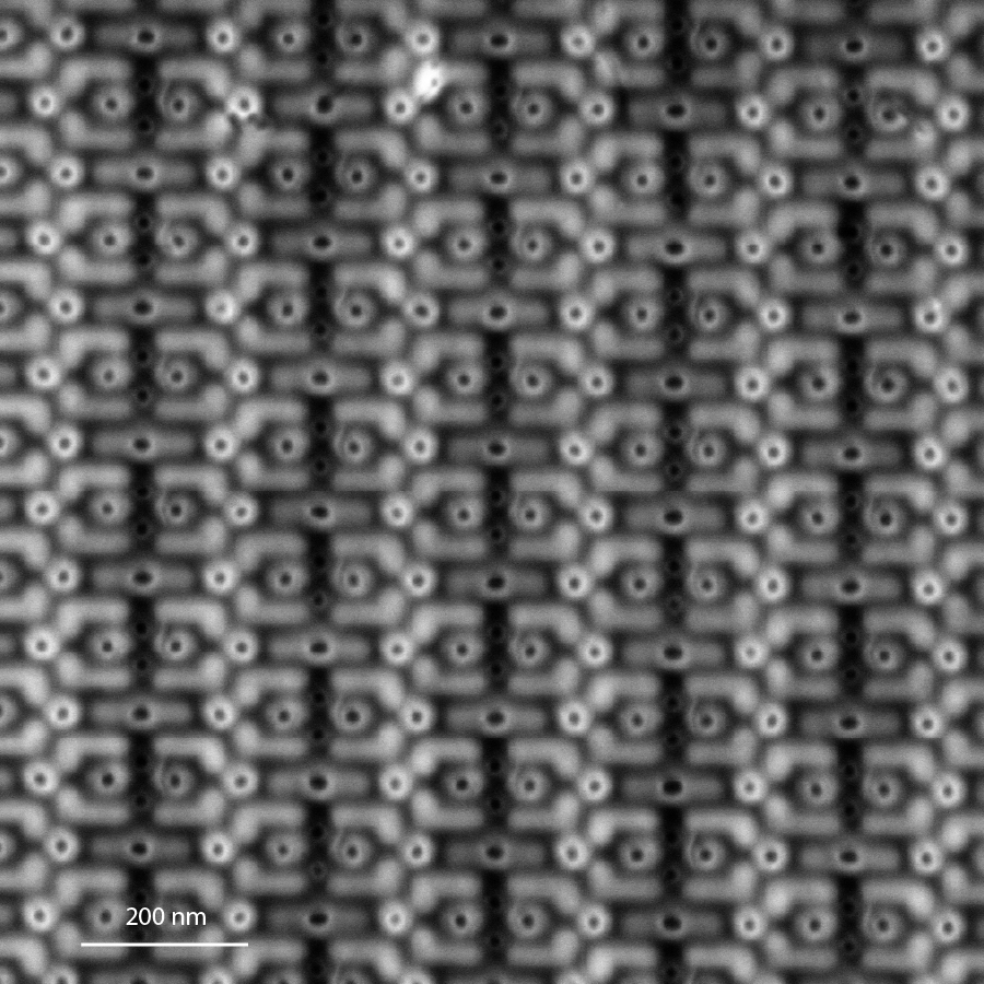
In this first session of the ZEISS Microscopy Defect Localization Webinar Series, we spotlight passive voltage contrast (PVC) techniques using ZEISS GeminiSEM. Attendees will explore three key mechanisms for generating PVC in devices, supported by practical examples in both electron and ion microscopy.
Participants will:
- Learn why defect localization is vital for semiconductor failure analysis.
- Explore three PVC mechanisms: capacitance, grounding, and the built-in potential of a p/n junction.
- Consider how the ability to select different energy distributions in ZEISS GeminiSEM enables accurate PVC.
- Get practical tips to optimize PVC techniques and your analysis results.


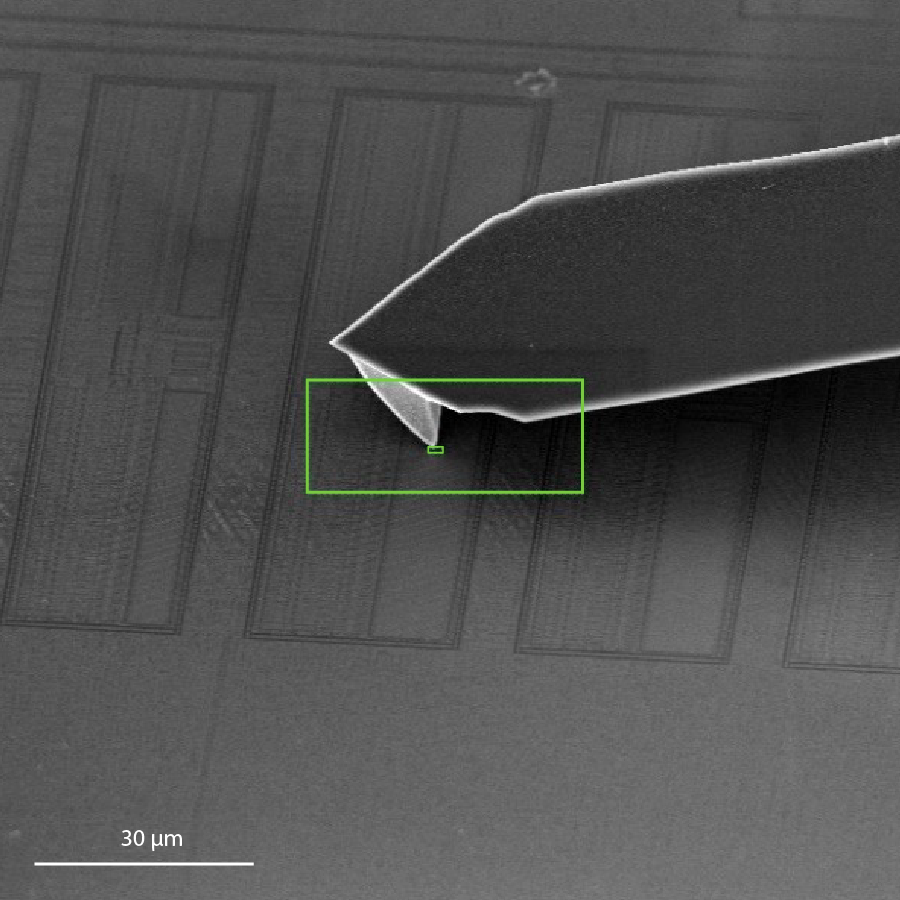
Nanoprobing: 10 Signals for Device Characterization & Defect Localization
In this session, we shift the focus to nanoprobing, introducing techniques such as current-voltage characterization, electron beam absorbed current (EBAC), electron beam induced current (EBIC), and electron beam induced resistance change (EBIRCH). Logic and power device applications will be presented, along with a case study on eDRAM shorts that illustrates nanoprobing's ability to uncover subtle defects, particularly in complex systems.
Participants will learn:
- The importance of localization for semiconductor failure analysis.
- The essential equipment, including SEM and nanoprobing systems, required for performing key electrical measurements like resistance and threshold voltage.
- The physics and uses cases for 10 different localization signals from nanoprobe-based analyses
- The challenges in finding shorts in complex systems.
- Nanoprobing’s ability to measure device health and localize a wide range of defects.

Conductive AFM: Big Insights from Tiny Places
In the final session, we will present the AFM-in-SEM system. This hybrid tool allows for high-resolution topographic and conductive measurements inside the scanning electron microscope (SEM.) Participants will learn about the usefulness of this tool for precise electrical measurements in tiny spaces inside the SEM. The ability to precisely detect electrical breakthroughs during localized milling will be demonstrated.
Four different aspects of the testing will be explored:
- Topographic measurements, the basic testing regime of AFMs.
- Conductive AFM measurements and the benefits of this system for SRAM analysis (AC bias on the backside with a linear filter).
- Electron beam absorbed current (EBAC) measurement with an AFM tip.
- Use of an AFM tip as a scalpel to clean oxidized surfaces or perform tomographic measurements (while simultaneously milling and collecting conductive AFM data).


Greg Johnson is a Senior Application Development Engineer in the Electronics Sector of ZEISS Microscopy and a senior IEEE member. With over 20 years of experience in semiconductor process development and failure analysis, Greg brings a wealth of experience to his role. Previously at IBM, he contributed to ceramic packaging process development and led FEOL defect localization efforts across multiple technology nodes, developing advanced failure analysis techniques. At ZEISS, Greg works with failure analysis engineers worldwide to advance SEM, FIB-SEM, and AFM techniques for semiconductor process development.


Dr. Sven Davani is the Market Sector Manager for Electronics at ZEISS, specializing in SEM and FIB-SEM technologies to tackle challenges in advanced semiconductor logic, memory, and packaging. He brings a customer-focused approach to driving technology adoption in the electronics industry. Before ZEISS, Sven worked in R&D consulting on innovation strategies and led product management in a startup, gaining experience in bringing new technologies to market. Sven holds a PhD in Physics from the University of Münster, with research in material science and microscopy published in journals like Acta Materialia and Ultramicroscopy.