ZEISS at ISTFA 2022
Pasadena, California, USA | Booth #805- 00 years
- 00 months
- 00 days
- 00 hours
- 00 minutes
- 00 seconds
Accelerate Failure Analysis for Next-generation Electronic Devices
New materials and semiconductor technologies are advancing the performance of next-generation electronics. Fast failure analysis becomes more important than ever for all stages of the product life cycle – from R&D to yield improvement to field returns.
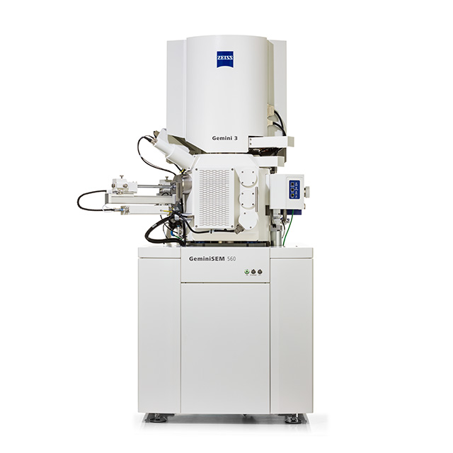
ZEISS offers advanced 3D imaging solutions for both front-end and back-end processes. Please visit our booth #805 at ISTFA to speak with our team about our unique X-ray, FE-SEM and FIB-SEM microscopy solutions for failure analysis and process development. Learn about our breakthrough Crossbeam laser “packaging FIB” for rapid nanoscale imaging of deeply buried features. See how Xradia 3D X-ray microscopes powered by artificial intelligence deliver faster scan times with images that look better than ever. Discover how our new GeminiSEM FE-SEM enables ultra-low voltage surface imaging and large field of view nanoprobing for your most demanding imaging and analytical tasks.
Tools of the Trade Tour – Monday, October 31
ZEISS is participating in the Tools of the Trade Tour on Monday night. Secure one of the limited slots in the Tour for a demonstration of ZEISS DeepRecon Pro, the industry’s first commercially available deep learning reconstruction technology in the 3D X-ray market. This new technology enables faster 3D X-ray scans while preserving ZEISS’s superior image quality.
ZEISS in the Technical Program
Sunday, October 30
Microscopy I & II Session – Ballroom C, 8:00 am PST
Tutorial – “Basics and Current Aspects of Scanning Electron Microscopy”
Dr. Heiko Stegmann, Carl Zeiss Microscopy GmbH
Fault Isolation I & II Session – Ballroom B, 11:20 am PST
Tutorial – “FA Technique Selection for Front End Defect Localization in Bulk Semiconductor (Si) FA"
Mr. Greg Johnson, Carl Zeiss Microscopy
Monday, October 31
Emerging FA Techniques and Concepts Session; Ballroom D, 10:20 am PST
Invited Talk - MultiSEM Applications in Failure Analysis and Fault Isolation of Semiconductors
Dr. Eugen Foca, Carl Zeiss SMT GmbH
FIB Sample Preparation Session – Ballroom B, 3:30 pm PST
“New Approach in Physical Failure Analysis Based on 3D Reconstruction”
Dr. Heiko Stegmann, Carl Zeiss Microscopy GmbH
Flavio Cognigni and Marco Rossi, Dept. of Basic and Applied Sciences for Engineering (SBAI), Centre for Nanotechnology Applied to Engineering of Sapienza (CNIS), Sapienza University of Rome, Italy
Co-authored with STMicroelectronics, presented by Dr. Domenico Mello
Tuesday, November 1
Industry Exchange – Standardized and AI Enhanced FA Workflows, Ballroom B, 10:55 am PST
“Concepts for Advanced Sample Holder and Data Exchange Interfaces”
Mr. Gabriel Reichl, Carl Zeiss Microscopy GmbH
Wednesday, November 2
Packaging and Assembly Level FA Session, Ballroom B, 10:00 am PST
“A Correlative Microscopic Workflow for Nanoscale Failure Analysis and Characterization of Advanced Electronics Packages”
Dr. Thomas Rodgers, Carl Zeiss Microscopy (co-authored with Fibics Incorporated and MCS Ltd)
Case Studies: Device Analysis Session, Ballroom A, 10:00 am PST
“Simple Methods for Evaluating Junctions in IGBTs”
Dr. Vignesh Viswanathan, Carl Zeiss Pte Ltd (co-authored with Kleindiek Nanotechnik, Ted Pella, and MCS Ltd)
Thursday, November 3
Microscopy and Material Analysis I Session, Ballroom B, 11:25 am PST
“Building a Better Lab Space for High Tech Imaging/Processing Tools”
Ms. Cheryl Hartfield, Carl Zeiss Microscopy (co-authored with S. Herschbein, Thermo Fisher Scientific and Intel)
Scanning Probe Analysis II Session, Ballroom A, 1:40 pm PST
“AFM in SEM for Device Characterization and Defect Localization”
Mr. Greg Johnson, Carl Zeiss Microscopy (co-authored with DoubleFox GmbH)
Microscopy and Material Analysis II Session, Ballroom B, 2:40 pm PST
“FIB-SIMS in FIB-SEMs: Practical Aspects for Physical Failure Analysis”
Dr. Heiko Stegmann, Carl Zeiss Microscopy GmbH (co-authored with TOFWERK AG)
Nanoprobing & Electrical Characterization Session, Ballroom B, 3:55 pm PST
“Zero Channel Bias Determination of Device Turn-on and the Seebeck Effect in Nanoprobing”
Mr. Greg Johnson, Carl Zeiss Microscopy (co-authored with Kleindiek Nanotechnik)
ZEISS Microscopy Solutions for Failure Analysis


ZEISS Xradia Versa X-ray Microscope
Image buried defects and package structures non-destructively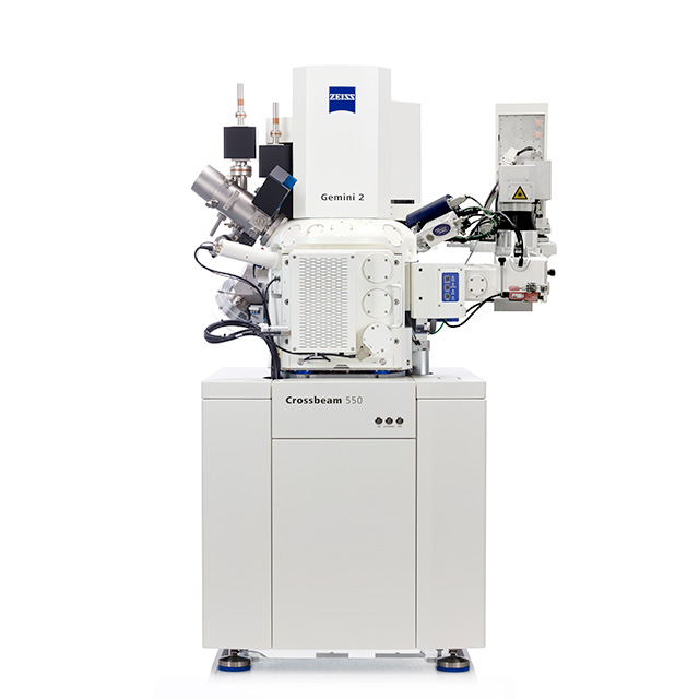

ZEISS Crossbeam laser FIB-SEM
Rapidly access site-specific features buried deeply within IC packages

ZEISS Crossbeam FIB-SEM
Achieve versatile, efficient imaging and processing for high-resolution 2D and 3D insights