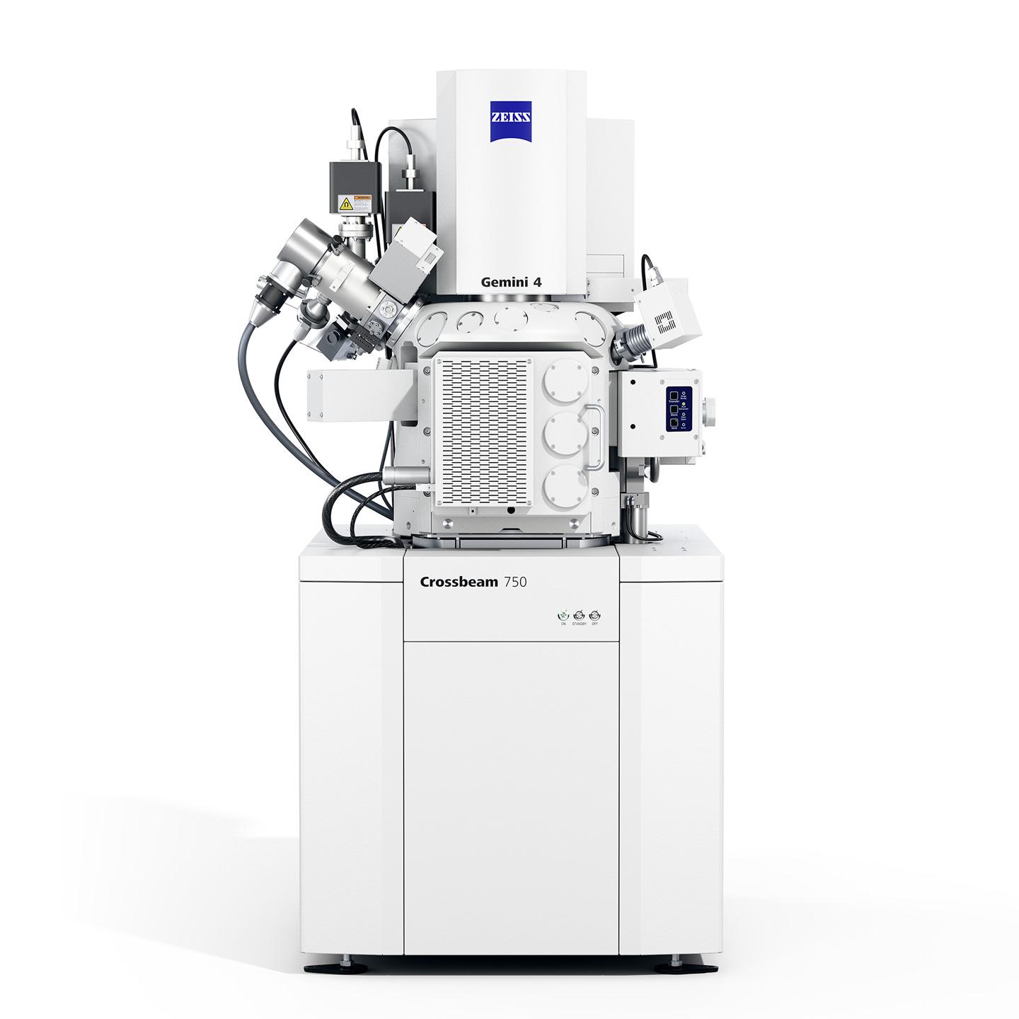
ZEISS GeminiSEM
FE-SEM For Highest Demands in Sub-nanometer Imaging, Analytics and Sample FlexibilityZEISS GeminiSEM stands for effortless imaging with sub-nanometer resolution. These FE-SEMs (field emission scanning electron microscope) combine excellence in imaging and analytics. Innovations in electron optics and a new chamber design let you benefit from better image quality, usability and flexibility. Take sub-nanometer images below 1 kV without an immersion lens. Discover three unique designs of the ZEISS Gemini electron optics.


GeminiSEM 360
Benefit from surface sensitive imaging and gather information at low voltage or at high probe current. Discover the advantages of Inlens detection, NanoVP, contextual image viewing or AI-powered segmentation.
Caption: Ferrocerium particle, Inlens EsB image.


Leverage comprehensive sample characterization with two unique Inlens detectors configured in parallel.
Your Tool for Sample Flexibility
✔ GeminiSEM 360 is the ideal instrument for a core facility, delivering maximum versatility for materials & life science, and industry.
✔ The eponymous electron optical design Gemini 1 brings you the benefit of surface sensitive, high resolution images providing excellent resolution at low voltage and great speed at high probe current.
✔ Gather high resolution, surface- and compositional information, even on sensitive samples by using Inlens secondary and backscatter electron imaging simultaneously.
✔ When aiming to image non-conducting samples under lower vacuum, so-called variable pressure, there is no need to forgo Inlens contrast: NanoVP guarantees maximum versatility enabling Inlens imaging without charging.


Configure your instrument tailored to your needs thanks to the versatile chamber.
Unrivalled User Experience
✔ GeminiSEM 360 delivers exceptional user experience: With its wide field of view and new, highly configurable chamber, it’s easy to interrogate even very large samples.
✔ Enjoy seamless navigation with contextual image viewing and correlative microscopy via ZEISS ZEN Connect.
✔ Gain clear, crisp images easily by using autofunctions e.g. the autofocus and smart detectors.
✔ Perform both imaging and analytical workflows efficiently with diametrically opposite EDS ports and a coplanar EDS/EBSD geometry.
✔ Maximize system uptime with ZEISS Predictive Service and benefit from scheduled maintenance to take place when you are ready.


Perform multimodal experiments with ZEN Connect and understand your specimens completely. (Particles of cathode material of a lithium ion battery, overlay of SEM and Raman.)
Exceptional Capability Extension
✔ Upgradability is essential for protecting your investment. That‘s why GeminiSEM 360 is plugged into the software ecosystem of ZEISS ZEN core.
✔ Draw on ZEN Connect to combine multimodal and multiscale data, ZEN Intellesis for advanced AI- powered segmentation, and ZEN’s analytical modules for reporting and analysis of segmented data. ZEN data storage lets you manage projects centrally by connecting data from different instruments in your lab.
✔ Access workflows and scripts created by other users who can help you solve challenges by being a member of the APEER community.
✔ Improve your system as new capabilities are released thanks to a clear upgrade ability path.


GeminiSEM 460
Switch seamlessly from low current-low kV work to high current-high kV work. Extend your possibilities with an in situ heating and tensile lab. Take advantage of a coplanar EDS/EBSD configuration, shadow-free mappings of EDS data and rapidly collecting EBSD maps with 4000 patterns/s.
Caption: Steel, EBSD map


Conduct rapid analysis and achieve high current and high resolution simultaneously. (EBSD map of a metal sample.)
Utilize High Resolution and High Current
✔ GeminiSEM 460 is made for your most exacting analytical tasks and enables efficient analysis and unattended workflows.
✔ Perform high-resolution imaging and analytics rapidly: switch seamlessly from low current-low kV work to high current-high kV work, and back again utilizing the Gemini 2 column.
✔ Characterize any specimen comprehensively by using multiple detectors in parallel.
✔ For efficient analysis exploit the versatile chamber and choose appropriate analytical detectors.
✔ Use the new VP mode and turn up the current to obtain EBSD maps with indexing rates of 4000 patterns/s.
✔ Investigate chemical composition and crystal orientation with two diametrically opposite EDS ports and a coplanar EDS/EBSD configuration. Count on high speed, shadow-free mapping.


Configure your instrument tailored to your needs thanks to the versatile chamber.
Customized, Automated Workflows
✔ With such powerful analytics at hand workflow automation becomes key. Create and configure automated experiments of your own with the Python scripting API from ZEISS.
✔ Modify experiments and customize the outcome to your own requirements.
✔ Make the most of STEM tomography: combine automated tilting and rotation with feature tracking. Produce 3D tomograms with nanometer-scale resolution after all aligned images are then sent to a proprietary 3D reconstruction software.
✔ When you need to test materials to their engineering limits, ZEISS puts an automated in situ heating and tension experimental lab at your disposal: it lets you observe materials under heat and tension automatically while plotting stress-strain curves on the fly.


Turn your GeminiSEM 460 into an in situ lab.
Your Pathway to Even More Possibilities
✔ Expand your analytical capabilities across materials and life sciences with exceptionally high, tunable current density, even at low kV - based on the Gemini 2 design.
✔ Take advantage of being able to adapt the system with a wide variety of accessories. The versatile chamber can be configured not only with analytical equipment but also with devices for in situ experiments, cryo-imaging and nanoprobing. storage lets you manage projects centrally by connecting data from different instruments in your lab.
✔ This lets you benefit from the ability to accommodate many configurations and upgrades at any point during the lifetime of your instrument.
✔ All GeminiSEMs are plugged into the ZEISS ZEN core ecosystem giving you access to ZEN Connect, ZEN Intellesis and ZEN’s analytical modules providing reporting and GxP workflows.


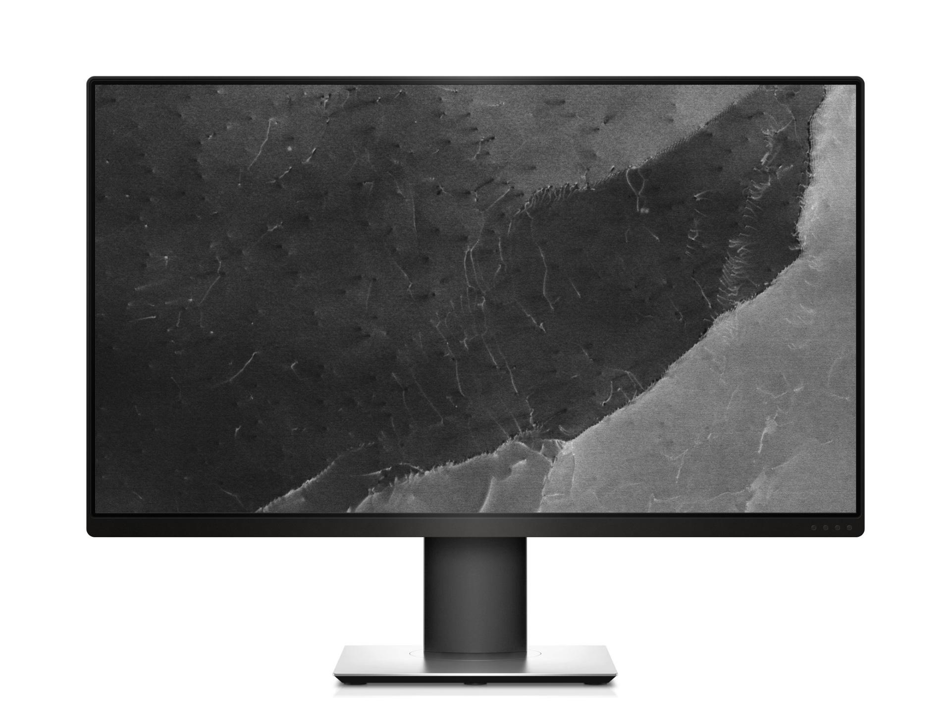
GeminiSEM 560
Explore the new standard for surface imaging: magnetic field-free imaging with sub 1 nm resolution below 1kV without sample biasing or monochromation, Gemini 3 with its new electron optical engine Smart Autopilot, finding the sweet spot in your working conditions – and much more.
Caption: Magnetic FeMn nanoparticles, edge length of a cube ca. 25 nm. GeminiSEM 560, 1 kV, Inlens SE, field of view 565 nm.


Details on the surface of a non-conducting mineral particle at low kV: GeminiSEM 560 at 800 V, Inlens SE.
Image Below 1kV Easily
✔ Gemini 3 enables magnetic field-free imaging with sub 1 nm resolution below 1 kV - without the need for sample biasing or monochromation. It includes the Nano-twin lens and the new electron optical engine Smart Autopilot.
✔ Achieve images of non-conducting matter with a new variable pressure mode and detection system: ensure fast results and preserve features by bringing vacuum-sensitive specimens into the chamber through the new Gentle Airlock in VP mode.
✔ Analyze delicate samples with ease by leveraging the new, large chamber with dual EDS ports. Produce fast, shadow-free mapping ensured by an optimum detector solid angle.


3D STEM tomography on a CeO2 nanoparticle. GeminiSEM 560, aSTEM, bright field, 30 kV.
Expert Knowledge Integrated
✔ Perform easy sample navigation by leveraging the greatly increased system’s field of view.
✔ Imaging of challenging samples is now accelerated by the new electron optical engine Smart Autopilot. It lets you save time while making lengthy alignments obsolete: the engine drives the electron optics to provide magnifications from less than 1× up to 500kx, taking care of alignment, calibration and focus along the way. A new patented parallax autofocus is included and a new auto-wobble provides you with clear, crisp images within seconds.
✔ Python scripting is able to use these features in automated workflows such as 3D STEM tomography.


A sweet spot: Magnetic contrast on a NdFeB magnet
Experience Unique Contrast
✔ Finding the sweet spot in your working conditions means that you’ve selected exactly the right combination of parameters to achieve the perfect image: the trick is finding it. Gemini technology with its magnetic field-free imaging and the new Gemini 3 column lets you find these sweet spots and discover new information.
✔ Magnetic contrast imaging is easy with a magnetic field on the sample of less than 2 mT. Perform energy spectroscopic imaging with the energy-selective Inlens back-scatter detector and electron angular spectroscopic imaging with the annular backscatter detector.
✔ Bring all your data together with ZEN Connect to segment and report on your findings.
Interview with Dr. Mario Hentschel


Dr. Mario Hentschel
Optical Sensors Research at the University Stuttgart, 4th Physics Institute and Center for Applied Quantum Technology, Germany.


"We are dealing with micro- and nanostructures for optical sensing. Consequently, it is important to characterize devices on a nanometer scale. These applications require a large flexibility of the electron microscope. ZEISS GeminiSEM 560 is offering us an astonishing degree of freedom and flexibility. We obtain highest quality images even from very challenging samples, such as highly insulating polymers, showing minimal effects due to charging. The GeminiSEM 560 will thus definitely be an enabling technology for our research which we feel that this instrument can provide it in a very flexible way."
The Technology Behind Gemini Electron Optics
-
What You Always Wanted to Know About the Fundamentals
Field emission SEMs are designed for high resolution imaging. Key to the performance of a field emission SEM is its electron optical column. Gemini is tailored for excellent resolution on any sample, especially at low accelerating voltages, for complete and efficient detection, and ease-of-use.


The Gemini 1 optical column consist of a beam booster, Inlens detectors and a Gemini objective.
Gemini optics are characterized by three main components:
- ● The Gemini objective lens design combines electrostatic and magnetic fields to maximize optical performance while reducing field influences at the sample to a minimum. This enables excellent imaging, even on challenging samples such as magnetic materials.
- ● Gemini beam booster technology, an integrated beam deceleration, guarantees small probe sizes and high signal-to-noise ratios.
- ● The Gemini Inlens detection concept ensures efficient signal detection by detecting secondary (SE) and backscattered (BSE) electrons in parallel minimizing time-to-image.


For your applications benefit from:
- ✔ Long-term stability of the SEM alignment and the effortless way it adjusts all system parameters such as probe current and acceleration voltage.
- ✔ Achieve distortion-free, high resolution imaging with the help of the near magnetic-field free optics.
- ✔ Get information solely from the top-most layer of your samples with the Inlens SE detector that produces images out of the truly surface sensitive SE 1 electrons.
- ✔ Obtain true material contrast at very low voltages with the detection concept of the Inlens EsB detector.
-
Capitalize on Fast Analytics
A comprehensive characterization of any sample calls for performance in imaging and in analytics. Plus, today’s users expect the set up and handling of the instrument to be easy. The Gemini 2 optics answers these demands.


Switch seamlessly between high resolution imaging and analytics
- ● GeminiSEM 460 comes with Gemini 2 optics featuring a double condenser.
- ● Adjust the beam current continuously while the spot size stays optimized simultaneously.
- ● Switch seamlessly between high resolution imaging – at low beam currents – and analytical modes – at high beam currents.
- ● You save time and effort because there’s no need to realign the beam after changing imaging parameters.


EBSD map of steel.
Stay flexible and work efficiently
- ✔ Stay flexible: use the highest beam current density for high resolution imaging and analysis at both low and high beam current, independently of which beam energy you select.
- ✔ Your specimen won’t be exposed to a magnetic field: achieve distortion-free EBSD patterns and high resolution imaging over a large field of view.
- ✔ Tilt the specimen without influencing the electron optical performance. Image even magnetic samples easily.
- ✔ Choose a charge reduction mode that suits your sample best: local charge compensation, variable pressure in the chamber or NanoVP.
-
Imaging below 1 kV - Expert Knowledge Integrated
The Gemini 3 optics are optimized for resolutions at low and very low voltages, and for contrast enhancement. They ensure maximum resolution at all working conditions from 1 kV to 30 kV and consists of two components which work synergistically: the Nano-twin lens and Smart Autopilot, a new electron optical engine. Additional technological characteristics are the high gun resolution mode and the optional Tandem decel.
Resolution Modes – Enabling You to See More Details
More details and more detection signal for your SEM images, enabled by two modes. In high resolution gun mode, the reduced energy spread of the primary beam minimizes the effect of chromatic aberration to allow even smaller probe sizes. In Tandem decel mode, a deceleration voltage is applied to the sample. Use this to further improve resolution below 1 kV and boost the detection efficiency of backscattered diode detectors.
, Smart Autopilot (blue).")
, Smart Autopilot (blue).")
The Nano-twin lens delivers:
- ● Sub-nanometer resolution at low and ultra-low voltages with excellent signal detection efficiency.
- ● Three times lower lens aberrations at low kV compared to the standard Gemini objective lens - resulting in a three times lower magnetic field on the sample, of the order of 1 mT.
- ● Optimized geometry and the electrostatic and magnetic field distributions.
- ● An enhanced Inlens detector signal under low voltage imaging conditions.
- ● These characteristics provide the ability for sub-nanometer imaging below 1 kV without immersing the sample in an electro-magnetic field.


The precision of the fine autofocus after 1 sec. focusing.
How it works:
- ● Smart Autopilot optimizes electron trajectories through the column thus ensuring the highest possible resolution at each acceleration voltage.
- ● The autofunctions enable a seamless alignment free transition across the entire magnification range from 1× to 2,000,000× and a 10× increase in the field of view allowing a 13 cm object to be imaged in a single frame.
- ● The image framestore of 32k × 24k in combination with the new overview mode ensure a stitching free pixel density over an unparalleled field of view


, Smart Autopilot (blue).")
, Smart Autopilot (blue).")


How-to Videos on Gemini Technology


Applications in Materials Science
Typical Tasks and Applications
- Image and analyze any real-world sample effortlessly, over large areas or at sub-nanometer resolution.
- Explore examples from nanoscience, engineering and energy materials, or bio-inspired materials, polymers & catalysts.
- See how GeminiSEM helps you to characterize your specimen comprehensively.
Caption: Structured gold platelets, research on plasmonic effects, GeminiSEM 560, BSD. Image: courtesy of University Stuttgart, Germany.
Nanoscience & Nanomaterials


Energy Materials


Engineering Materials
 and after loading (right).")
 and after loading (right).")
 and after loading (right).")
 and after loading (right).")
Stainless Steel - in situ tensile load test
A stainless-steel sample imaged under in situ tensile load test. Using the AsB detector, images have extremely high contrast and capture the slip bands formation during in situ loading as shown in the images of before (left) and after loading (right).
 and at 1 kV landing energy with 5 kV bias (right), providing enhanced material contrast and sharpness.")
 and at 1 kV landing energy with 5 kV bias (right), providing enhanced material contrast and sharpness.")
 and at 1 kV landing energy with 5 kV bias (right), providing enhanced material contrast and sharpness.")
 and at 1 kV landing energy with 5 kV bias (right), providing enhanced material contrast and sharpness.")
Nanocomposite Powder
Imaged with the BSE detector at 1 kV landing energy with no bias (left) and at 1 kV landing energy with 5 kV bias (right), providing enhanced material contrast and sharpness.
 versus a closer working distance of 1 mm (right).")
 versus a closer working distance of 1 mm (right).")
 versus a closer working distance of 1 mm (right).")
 versus a closer working distance of 1 mm (right).")
Stainless-Steel Surface
After surface preparation using sand blasting. The crushed SiO2 shows positive charging on the left image. Contrast visible only at large working distance of 5 mm (left) versus a closer working distance of 1 mm (right).
Bio-inspired Materials, Polymers & Catalysts


Microscopy Solutions for Industry
Typical Tasks and Applications
- Failure analysis on mechanical, optical or electronic components
- Fracture analysis and metallography
- Surface, microstructure and device characterization
- Compositional and phase distribution
- Impurity and inclusion determination
Caption: Cross-section of lithium ion battery.
Steel and Batteries


Fracture surface – brittle failure of a steel sample in tension
Fracture surface – brittle failure of a steel sample in tension


Inclusions in steel, Inlens SE detector, 500 V
Inclusions in steel, Inlens SE detector, 500 V


EDS compositional mapping shows main constituents of the different oxides. Sample: courtesy of Aalen University, Germany.
Lithium ion battery cathode
 shows deeply-buried structures such as FinFET gates, tungsten plugs, and tin liner (inset) with exceptional resolution and contrast.")
 shows deeply-buried structures such as FinFET gates, tungsten plugs, and tin liner (inset) with exceptional resolution and contrast.")
Applications in Electronics & Semiconductor
Typical Tasks and Applications
- Construction analysis and benchmarking
- Passive voltage contrast
- Subsurface analysis
- Electronic property measurement with probing
- TEM site selection
Caption: The aBSD detector at high EHT (here at 30 kV ) shows deeply-buried structures such as FinFET gates, tungsten plugs, and tin liner (inset) with exceptional resolution and contrast.
Electron Beam Absorbed Current (EBAC)
Probing during imaging can give further insight into function. Here, electron beam absorbed current (EBAC) shows the connectivity of a circuit with a probe tip landed at one node.


 and thus guide failure analysis for the TEM workflow, aBSD detector at 30 kV.")
 and thus guide failure analysis for the TEM workflow, aBSD detector at 30 kV.")
 and thus guide failure analysis for the TEM workflow, aBSD detector at 30 kV.")
 and thus guide failure analysis for the TEM workflow, aBSD detector at 30 kV.")
FinFET Gates
Backscatter images show deeply-buried structures such as FinFET gates, tungsten plugs, and tin liner (inset) and thus guide failure analysis for the TEM workflow, aBSD detector at 30 kV.


Applications in Life Sciences
Typical Tasks and Applications
- Characterization of topology
- Imaging sensitive, non-conductive, outgassing, or low contrast samples
- Visualizing the ultrastructure of cells, tissues etc. at high resolutions
- Imaging very large areas such as serial sections or block faces
Caption: SARS-CoV-2 virus, culture, inactivated, negatively stained, GeminiSEM 560, aSTEM, HAADF/BF. Sample: courtesy of M. Hannah, Public Health England, UK.


SARS-CoV-2 virus
SARS-CoV-2 virus, culture, inactivated, negatively stained, GeminiSEM 560, aSTEM, HAADF/BF. Sample: courtesy of M. Hannah, Public Health England, UK.


Mouse Brain
Applying Tandem decel increases contrast to such an extent that cell organelles are clearly visible at high resolution, mouse brain. Sample: courtesy of C. Genoud, FMI, Basel, CH.
Root Nodules of Fabaceae Beans
Investigate large areas with array tomography, serial section & block face Imaging. Root nodules of Fabaceae beans, imaged with ZEISS Atlas 5, 78 sections.
Accessories

TEM-like Defect Imaging with cECCI
Image crystallographic defects using controlled Electron Channeling Contrast Imaging (cECCI) on your ZEISS GeminiSEM. Characterize deformations in bulk samples quantitatively without the need for a TEM. You can skip the tedious step for lamella preparation which is mandatory for TEM workflows and go beyond the one-shot analysis approach. You will not only acquire excellent images of defects with ease and minimal sample preparation. But you can also benefit from having access to true sample representivity. Configure your GeminiSEM 460 or 560 with a sensitive backscatter detector, a precise 6-axis stage, EBSD analytics and the TOCA (Tool for Orientation and Crystallographic Analysis) software. Determine the perfect imaging conditions. Control the illumination of the crystal lattice by educated tilting of your sample to achieve the two-beam condition or the invisibility criterion and perform electron channeling contrast imaging on your SEM. Visualize and measure crystallographic defects such as dislocations, stacking faults and twin boundaries crucial to materials science research on TEM-like images of superior quality.
3D STEM Tomography
Automated STEM tomography on an FE-SEM is now put at your disposal. A script for automated acquisition of a STEM tilt series uses the API and performs compucentric, rotation and tilt stage movements as well as autofocus and image acquisition. Feature tracking compensates for shifts throughout the entire tilt series and keeps the drift between two images to a minimum of around 50 nm. The STEM sample holder allows to tilt the stage to 60° and to perform a 180° rotation, and the aSTEM detector covers all requirements. From the advanced reconstruction toolkit (ART) development team, 3D reconstruction software then takes this output and renders a 3D model of your sample.


Sample courtesy of Christel Genoud, Université de Lausanne, Switzerland
Sample courtesy of Christel Genoud, Université de Lausanne, Switzerland
In-Chamber Ultramicrotome for Serial Block-Face SEM
Image the ultrastructure of biological, resin-embedded samples in 3D over large areas. ZEISS Volutome is an end-to-end solution from hardware to software including image processing, segmentation, and visualization.
ZEN core for EM
New SEM Control Software and Entry to Connected MicroscopyBenefit from this software that is more than just a system control: ZEN core is your single, standardized user interface for basic control of ZEISS SEMs and FIB-SEMs. It introduces intuitive, streamlined imaging, and analytics, and lets you perform correlative, multimodal workflows.
Your key features are:
- Easy SEM operation
- Integration of SEM imaging and EDS analysis
- Unique entry point to the ZEN core ecosystem
- Control of basic FIB-SEM workflows including automated multi-site TEM lamella preparation


Link Materials Performance to Microstructure with the In Situ Lab for ZEISS FE-SEMs
Benefit from an Integrated SolutionExtend your ZEISS FE-SEM with an in situ solution for heating and tensile experiments. Investigate materials like metals, alloys, polymers, plastics, composites, and ceramics. Combine a mechanical tensile or compression stage, a heating unit and dedicated high-temperature detectors with analytics. Control all system components from a single PC with a unified software environment that enables unattended automated materials testing.


Visualization and Analysis Software
ZEISS Recommends Dragonfly ProAn advanced analysis and visualization software solution for your 3D data acquired by a variety of technologies including X-ray, FIB-SEM, SEM and helium ion microscopy. Available exclusively through ZEISS, ORS Dragonfly Pro offers an intuitive, complete, and customizable toolkit for visualization and analysis of large 3D grayscale data. Dragonfly Pro allows for navigation, annotation, creation of media files, including video production, of your 3D data. Perform image processing, segmentation, and object analysis to quantify your results.


")
")


")
")