Photonics
Helping You Advance Nanophotonics Research With Sub-10 nm Fabrication Capabilities and High-Resolution, Low-kV ImagingAccording to the European Commission website, “we are on the verge of a new photonics era”. This statement is not surprising given that photonics is considered one of Europe’s “key enabling technologies”. Not only this, but the field has produced many breakthroughs that have changed the way we live our lives.
A New Era of Photonics
But fabricating future nanoscale devices is becoming more challenging as Moore’s law approaches its limit. As a result of effects like quantum mechanical tunneling, scientists are unable to make these devices smaller. Instead, by studying different materials and technology - such as stacking transistors vertically (like in 3D NAND) - research can provide the processing power needed for these applications going forward.
Nanomaterials for photonics applications take the form of thin films, nanowires, quantum dots, and other low-D structures. The optical properties of these materials depend on their exact size, dimensions, and crystallinity. For example, single crystalline materials will typically show lower plasmonic losses than their polycrystalline counterparts. This has driven the fabrication of single crystal metal devices for plasmonics.
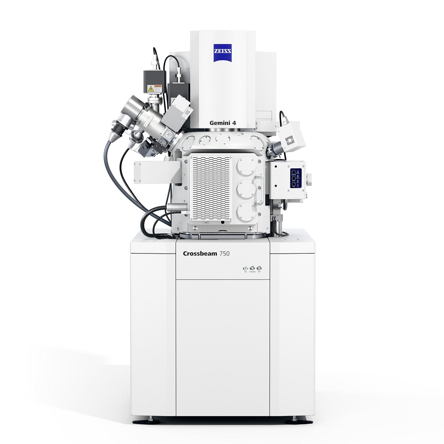
Dedicated Tools Are Needed to Push Photonics Further
These low-D materials for photonics applications need specialized tools to study their structure, chemistry, and physical properties. Also, high spatial precision is needed during fabrication. But standard SEM systems come with limitations, including poor resolution at low kV, as well as charging effects and beam induced sample damage. And fabricating structures using a standard Ga-ion FIB produces feature sizes on the order of 50 nm - too large to take advantage of quantum confinement effects.
ZEISS Workflows Can Help
To solve these challenges, you need tools that give you high performance, sub-10 nm imaging at low-kV. You also need to be able to deposit or fabricate structures at the same length scales to take advantage of quantum confinement. ZEISS Microscopy offers powerful correlative workflows that help you pattern sub-10 nm structures with high fidelity and image their surfaces at high resolution - without beam damage. Also STEM in SEM offers you impressive capabilities with a resolution down to 0.4nm. Moreover, STEM tomography is now available in SEM, bridging the gap to TEM and adding a new ease of use dimension.