A Greener Future
The Push for Low-Cost, Efficient Solar Cell TechnologyClimate change and recent weather extremes mean that green technology is now more crucial than ever. Development of novel, low-cost solar cell devices that maximize efficiency is critical if mankind is to reach net-zero emission by 2050. But several challenges need to be solved before this becomes a reality.
The first challenge is finding better materials for solar cell devices
For example, traditional silicon panels are bulky and inefficient. Perovskites, on the other hand, can improve efficiency, as they can be made with very thin layers and need less material overall. Another problem is boosting cell lifetime and improving durability - features that relate to the properties of a chosen material.
These properties, along with the performance of future photovoltaic devices, depend on the chemical and microstructural environments present. But creating and controlling these environments is incredibly challenging.
Materials scientists strive to understand the links between performance, structure, and processing so they can advance these technologies to meet our growing energy needs.
The need for better microscopy tools
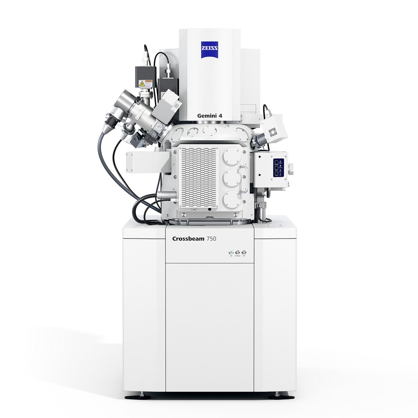
This is where microscopy can play a significant role in shaping the solar cells of the future. Correlative electron and ion microscopy can help you image features on multiple length scales at high resolution. At the same time, precise chemical analysis can be carried out using energy dispersive x-ray spectroscopy (EDS), while secondary ion mass spectrometry (SIMS) can accurately detect trace elements on a material’s surface. All of these techniques can provide you with the means necessary to develop and understand novel solar cell designs.
ZEISS offers correlative electron and ion microscopy solutions
These solutions provide the detailed analytical information needed by today’s researchers. ZEISS microscopes help you quickly and easily determine the chemical and structural environments in thin film, single-, and poly-crystalline solar cells. You can image beam sensitive materials like perovskites with the low-voltage imaging capabilities of Gemini optics, trace element distributions at the highest resolution using SIMS imaging, and efficiently analyze elemental distributions in 2D and 3D with EDS.
Your Next Step
Learn about the microscopy portfolio and about how ZEISS can help you push your solar cell research forward.
Application Images


Surface of a CIGS solar cell on an alumina substrate
Imaged with GeminiSEM at 1.8 kV using the Inlens SE detector to highlight the surface topography.