Dr. Sina Shahbazmohamadi customer profile
Little things. big impact.

Dr. Sina Shahbazmohamadi

Engineering the future. One micron at a time.

Assistant professor  |  University of Connecticut

Where microscopy meets manufacturing innovation.

Dr. Sina Shahbazmohamadi specializes in correlative microscopy and 3D imaging. Recently he’s applied his diverse skillset to develop new testing methods for electrical components across a variety of manufacturing fields.

About Dr. Shahbazmohamadi

  • Years of experience

  • Awards

Breakthroughs by Dr. Shahbazmohamadi

Medical device coatings

Serious as a heart attack.

Implantable medical devices like pacemakers and neurostimulators use specialized coatings that safely facilitate transfer of electrical charges. Since reliability is paramount, verifying the integrity of the coating microstructure is crucial.

Dr. Sina Shahbazmohamadi and team have designed a process where the use of non destructive 3D X-ray tomography, in conjunction with a Focused Ion Beam Scanning Electron Microscope (FIB SEM), work together to target and tomographically image a specific region of a device at the nanoscale.

The ZEISS Crossbeam provides a detailed 3D map of coating cracks or defects. The testing is crucial to mitigating the dire outcomes from failure of these devices.

From Dr. Shahbazmohamadi's lab

  • Surface roughness determined by laser scanning confocal microscopy.

    Surface characterization

    Surface roughness determined by laser scanning confocal microscopy.

  • Multiscale analysis of coatings

    Multiscale analysis of coatings

    Optical imaging and X-ray microscopy were used to determine roughness and irregularities in the coating interface, targeting a specific region of interest for high resolution 3D tomography with the FIB SEM.

Breakthroughs by Dr. Shahbazmohamadi

Navigating with connected microscopes

Finding the needle in a haystack.

A major challenge in materials characterization is to interrogate microscopic details from a single spot with an unknown location in a comparatively enormous component. This challenge is acute in the
world of microelectronics such as multilayer ceramic capacitors (MLCCs).It first requires location, then precise navigation, then observation.

Microscopes excel in different length scales, so finding the needle in a haystack relies on multiple instruments that work well together. Dr. Sina Shahbazmohamadi begins with XRM to establish a 3D roadmap of devices like MLCCs. This roughly gets to a region of interest. He then moves to the Crossbeam FIB SEM to target and characterize failures or identify potential counterfeit components.


From Dr. Shahbazmohamadi's lab

  • A femtosecond laser was user to access the anomalous region in the MLCC that was seen by Xray microscopy.

    Visualizing defects with FIB SEM

    A femtosecond laser was user to access the anomalous region in the MLCC that was seen by Xray microscopy. The region was then characterized
    by FIB slicing, SEM imaging and EDS mapping to visualize an enlargement and void spaces in the nickel plates.

  • Virtual view inside the MLCC

    Virtual view inside the MLCC

    X-ray microscopy allows researchers to inspect the inside of the device for voids or defects prior to cutting it open.

  • Inspection of the 3D XRM data revealed an anomalous region in one of the MLCC nickel plate layers

    Needle in a haystack

    Quick inspection of the 3D XRM data revealed an anomalous region in one of the MLCC nickel plate layers, which was then targeted for high resolution FIB SEM analysis.

Breakthroughs by Dr. Shahbazmohamadi

Understanding failures at microscale

Testing that raises the bar.

Failure in vital microelectronic components creates huge challenges. Microscopic characterization methods are critical to understanding the root cause of failures in order to design better materials andmanufacturing processes.

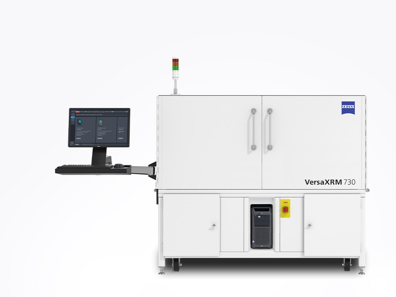
Dr. Shahbazmohamadi is developing enhanced microscopy techniques to understand these material breakdowns. Recently, his lab established the use of X-ray microcopy to capture bond wire geometries, perform image processing and then computer simulation.

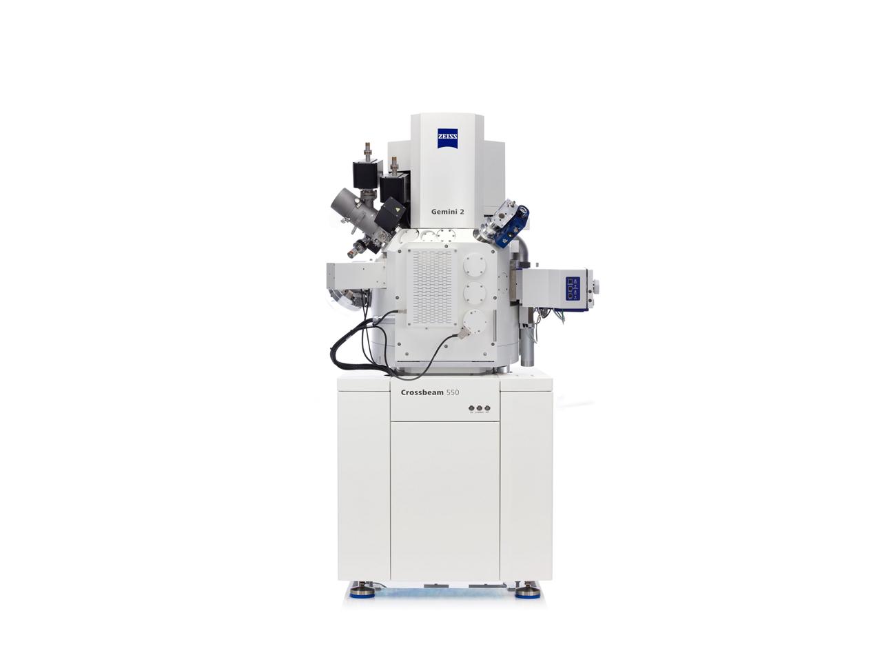
The lab developed an in situ testing device within the FIB SEM to observe mechanical deformation at the micro and nanoscale. By combining in situ testing with multiscale microscopy techniques, he is better able to identify potential device failures.


From Dr. Shahbazmohamadi's lab

  • Preparing bond wires for testing

    Preparing bond wires for testing

    Several bond wires are viewed in the FIB SEM after a short pulse laser has been used to decapsulate the package molding compound.

  • Preparing bond wires for testing

    Preparing bond wires for testing

    A closer look at bond wires prior to in situ pull testing in the FIB SEM.

  • Microelectronics in 3D

    Microelectronics in 3D

    3D X-ray microscopy data showing bond wire interconnects in a microelectronic device.

When we don't see what we are looking for, we don't give up. Instead, we REFINE our resolution.

Dr. Sina Shahbazmohamadi University of Connecticut

Shop Microscopes Online

Precision at your fingertips.

Accelerate your research with ZEISS top-class confocal microscopes, now available online with just one click.


Comprehensive Solutions and Capabilities

Discover Our Application Hub

Explore applications to discover tailored solutions for your unique laboratory needs and elevate your research capabilities.