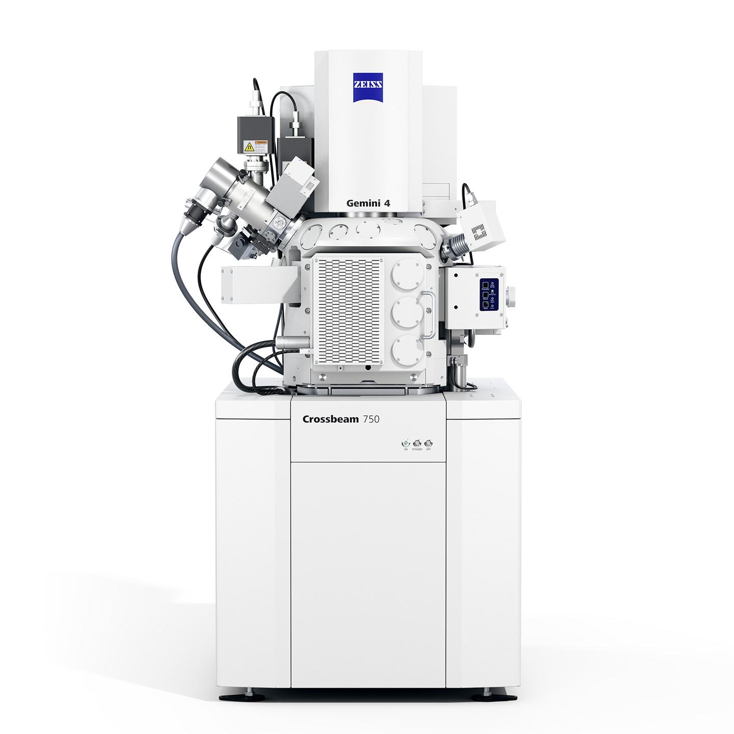
Semiconductor Device Development and Failure Analysis
Better Productivity for Complex Structural and Electrical CharacterizationSemiconductor products serve the needs of transportation, work, social communication, and industrial infrastructure. There is constant demand for higher computing performance in ever smaller form factors. Logic and memory semiconductor structure analysis is challenged by novel materials and increasingly complex geometries. Shrinking transistor sizes at the newest technology nodes demand the highest performance for electron microscopy and nanoprobing applications.


FIB-SEM Tomography of 3D NAND
FIB-SEM tomography of a 3D NAND sample acquired using ZEISS Crossbeam 550 and Atlas-3D. Sample was depackaged and mechanically polished down to the topmost word line. Shown is a virtual sub-volume of 2 x 1.5 x 0.7 µm3 size, extracted from the dataset at the transition region of upper to lower deck. Reconstructed voxel size 4 x 4 x 4 nm3.
The resulting reconstruction allows for looking at multiple planes of section across the device from any virtual section.
FIB-SEM 3D Tomography of 7 nm SRAM
3D FIB-SEM tomography dataset of a 7 nm SRAM, acquired in a ZEISS Crossbeam FIB-SEM.
Volume size 2.34 x 1.18 x 2.35 µm3, voxel size (1.5 nm)3.
The resulting reconstruction allows looking at multiple planes of section to find defects or assess process uniformity.


FIB-SEM Cross Section of 7 nm SRAM
SEM image of a corner FIB cut into a 7 nm SRAM. FIB milling and SEM imaging were done in a ZEISS Crossbeam FIB-SEM.
Fast cross sectioning with nanometer precision and highest quality combined with high-resolution imaging make Crossbeam a versatile tool for cross-sectional inspection of the most recent technology nodes structures.


TEM Prep - 7 nm SRAM
30 kV STEM bright field overview image of a plan view lamella of a 7 nm technology node processor at contact level. Lamella preparation and STEM imaging were done in a ZEISS Crossbeam FIB-SEM.
Inset: A STEM bright field image at high magnification shows the FinFETs in detail and allows to assess process variations.


Ultra Low-k Film Stack Imaging
Mechanical polished section of the same field of view in a 14 nm device imaged with a GeminiSEM FE-SEM.
Left:
The SE2 image highlights topological features, showing exposed vias.
Right:
The InLens image demonstrates the passive voltage contrast of areas which are connected to different depths of circuitry or connected to structures of different implant polarity.


7 nm SRAM Imaging with SenseBSD
Same field of view of a mechanical polished 7 nm SRAM, imaged at 1 kV in a GeminiSEM FE-SEM.
Left:
The Inlens image provides surface detail and highlights the passive voltage contrast between contacts of different types in the SRAM structure.
Right:
The SenseBSD image provides a mixture of Z contrast and topography contrast.


22 nm SRAM
22 nm SRAM
Ultra Low-kV Imaging of 7 nm SRAM
7 nm SRAM device imaged with a GeminiSEM FE-SEM at 80 eV. The superior resolution and magnetic-distortion-free imaging provided by the Gemini column are key to navigation and probe landing in nanoprobing.


Logic Tracing with EBAC
Net trace in a 14 nm SRAM imaged in a GeminiSEM FE-SEM with the Electron Beam Absorbed Current (EBAC) method. Images are an overlay of EBAC data (red) on top of the InLens image for the same field of view, at 2 kV (left) and 8 kV (right). Different acceleration potentials allow exploring different depths in the sample, thus tracing the full connective path.
Left: 2 kV
Right: 8 kV


EBIC Analysis of 7 nm SRAM
7 nm SRAM mechanically polished to contact level. The InLens (left) and Electron Beam Induced Current (EBIC) (right) images are compared for the same field of view, taken at 150 eV in a GeminiSEM FE-SEM. The use of EBIC can monitor p/n junction health and localize areas with electrically active defects.


EBIRCH Localization on 22 nm SRAM
22 nm SRAM mechanically polished to contact level. A short was intentionally created in the sample. Using the stable electron beam from the GeminiSEM FE-SEM, the sample was then imaged with Electron Beam Induced Resistance Change (EBIRCH) with only 12 nA flowing across the device during analysis. Both fins in a two-fin pulldown device are imaged..