
ZEISS at ISTFA 2025
Pasadena, California, USA | Booth #619- 00 years
- 00 months
- 00 days
- 00 hours
- 00 minutes
- 00 seconds
Come See What's New at ZEISS!
Stop by booth #619 to learn about the latest advances in 3D X-ray microscopy, FE-SEM, and FIB-SEM solutions for failure analysis and process development.
ZEISS has an exciting array of presentations, papers, and new products to share at ISTFA. Learn about correlative microscopy for hybrid bond FA, low impact analysis of junctions in power devices, AI image segmentation to characterize bond bads, automation, and more. Attend tutorials on SEM basics and defect localization for enhanced yield.
ZEISS in the Technical Program
Sunday, November 16
Tutorial – Basics and Current Aspects of Scanning Electron Microscopy
Session: Microscopy – SEM Basics – 11:20 am PST
Dr. Heiko Stegmann, Carl Zeiss Microscopy GmbH
Tutorial - Defect Localization Methods for Device Characterization and Yield Management
Session: CSAM II – 1:30 pm PST
Greg Johnson, ZEISS Microscopy
Monday, November 17
First and Preliminary Approach at the Usage of FIB ToF for Borophosphilicate Layer Characterization Directly on Device Failing Structures
Session: Microscopy Analysis and Material Characterization I – 1:40 pm PST
Dr. Domenico Mello, EM Microelectronic, a Company of the Swatch Group; Dr. Clement Huguenot, EM Microelectronic, a Company of the Swatch Group; Dr. Guillaume Fiannaca, EM Microelectronic, a Company of the Swatch Group; Dr. Heiko Stegmann, Carl Zeiss Microscopy GmbH; Dr. Hubert Schulz, Carl Zeiss Microscopy GmbH; Dr. Giuseppe D'Arrigo, CNR-IMM, CNR (Consiglio Nazionale delle Ricerche)
Correlative X-ray Nanotomography and FIB-SEM Microscopy for Hybrid Bond Failure Analysis
Session: Package Level Fault Isolation – 2:00 pm PST
Dr. Allen Gu, ZEISS Microscopy
Tuesday, November 18
AI-based Image Segmentation for the Characterization of Bond Pads after SLAT
Session: AI Applications for Failure Analysis II – 12:50 am PST
Mr. Dirk Utess, GlobalFoundries; Dr. Martin Weisheit, GlobalFoundries; Dr. Heiko Stegmann, Carl Zeiss Microscopy GmbH
Advanced Method for 3D FIB Tomography AI Supported on SRAM I/O Circuit Block with Missing Data Bits Problems
Session: AI Applications for Failure Analysis II – 1:30 pm PST
Dr. Domenico Mello, EM Microelectronic, a Company of the Swatch Group; Dr. Guillaume Fiannaca, EM Microelectronic, a Company of the Swatch Group; Dr. Filippo Marinelli, EM Microelectronic, a Company of the Swatch Group; Dr. Heiko Stegmann, Carl Zeiss Microscopy GmbH; Dr. Flavio Cognigni, Carl Zeiss SpA; Dr. Giulio Lamedica, Carl Zeiss SpA; Ms. Angelica Accorinti, University of Rome "la Sapienza"; Prof. Marco Rossi, Sapienza University of Rome
A Step Towards Automation in Failure Analysis by FIB-SEM 3D Tomography and AI Segmentation
Session: AI Applications for Failure Analysis II – 1:50 pm PST
Mr. Pascal Limbecker, GlobalFoundries Dresden Module One LLC & Co. KG; Dr. Heiko Stegmann, Carl Zeiss Microscopy GmbH; Dr. Rong Wu, GlobalFoundries Dresden Module One LLC & Co. KG; Dr. Daniel Plencner, Carl Zeiss Microscopy GmbH; Mr. Roland Salzer, Carl Zeiss Microscopy GmbH
Wednesday, November 19
Low Impact Analysis of Junctions in Power Devices
Session: Power Devices (Si, SiC, GaN) – 8:20 am PST
Mr. Greg Johnson, Carl Zeiss Microscopy; Mr. Andreas Rummel, Kleindiek Nanotechnik GmbH; Dr. Heiko Stegmann, Carl Zeiss Microscopy GmbH; Ms. Hyun Hwa Kim, Carl Zeiss Microscopy; N/A Leslie McCluskey, Ted Pella, Inc.; Dr. Jake R. Jokisaari, PhD, Ted Pella, Inc.
Microscopy Analysis and Material Characterization - ECCI imaging of epitaxial GaN with conventional FE-SEM
Poster Sessions – 3:00 pm PST
Ms. Hyun Hwa Kim, Carl Zeiss Microscopy; Mr. Greg Johnson, Carl Zeiss Microscopy; Dr. Thomas Rodgers, Carl Zeiss Microscopy
ZEISS Microscopy Solutions for Failure Analysis
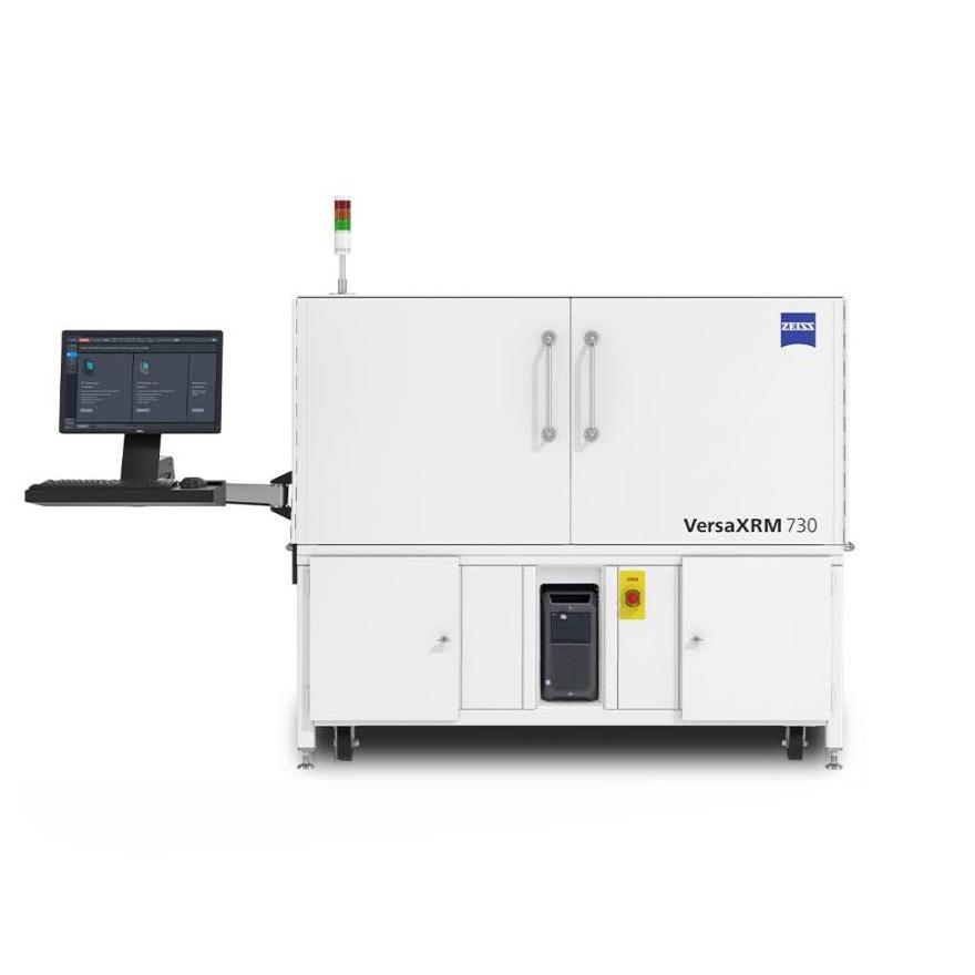

ZEISS Versa XRM X-ray Microscope
Image buried defects and package structures non-destructively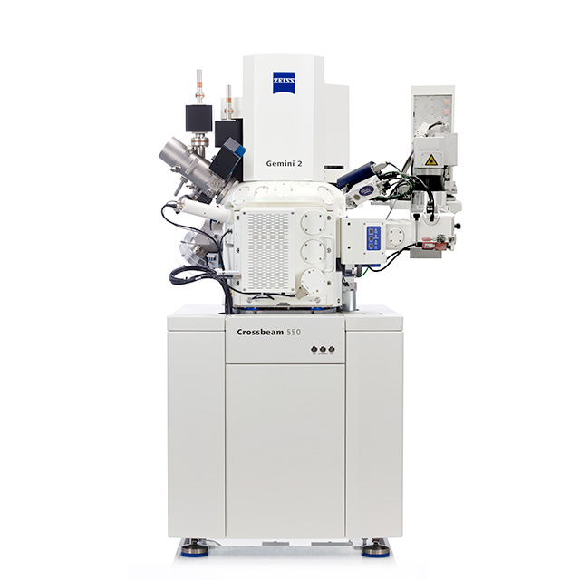

ZEISS Crossbeam laser FIB-SEM
Rapidly access site-specific features buried deeply within IC packages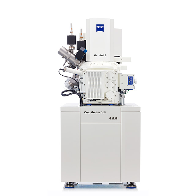

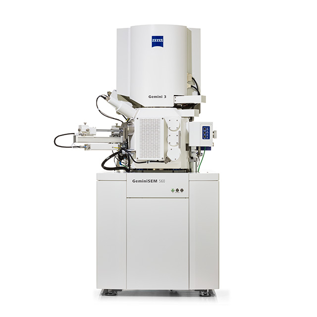
ZEISS Crossbeam FIB-SEM
Achieve versatile, efficient imaging and processing for high-resolution 2D and 3D insights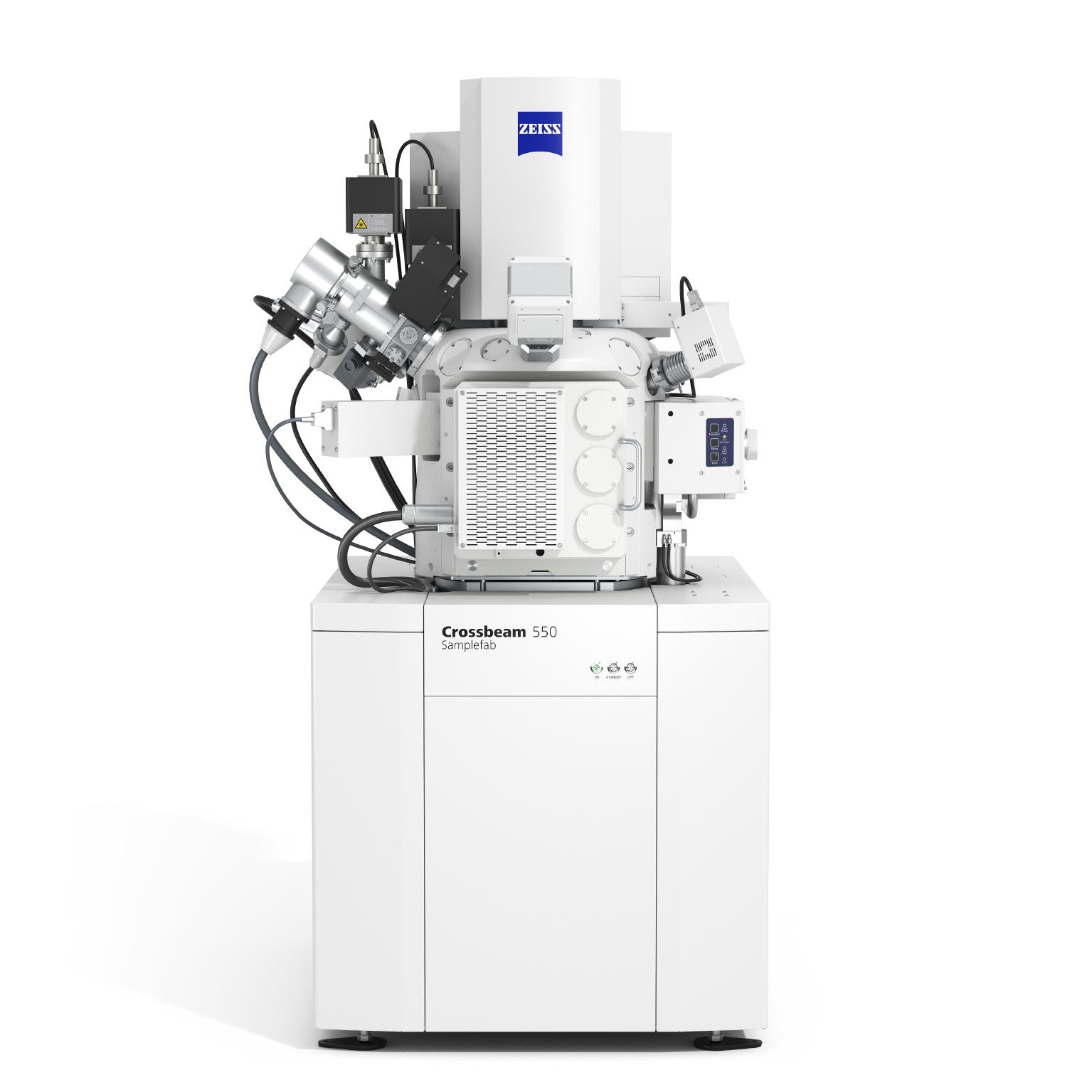

ZEISS Crossbeam Samplefab
Simplify sample preparation with fully-automated TEM lamella prep workflow