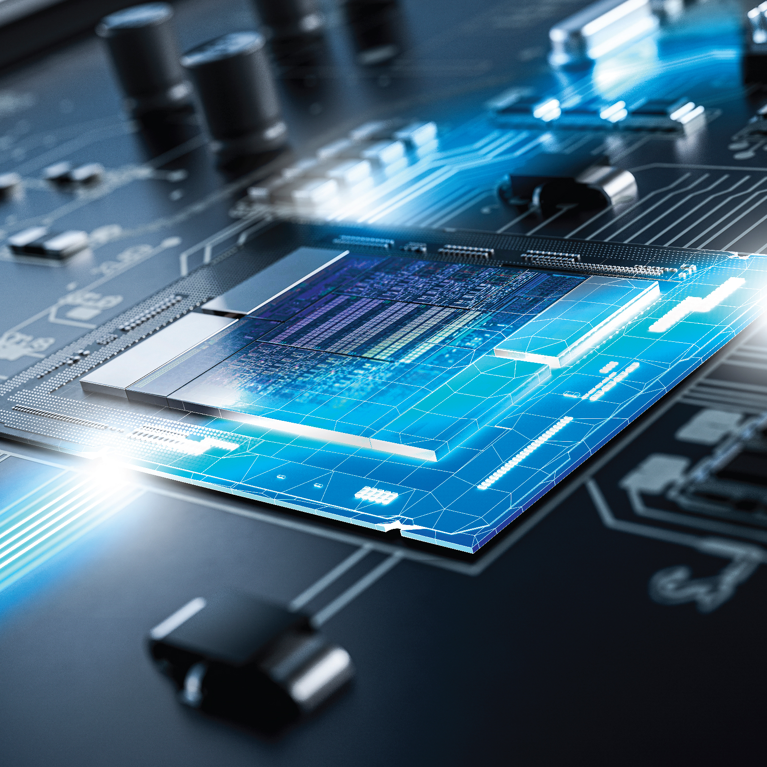

ZEISS at ISTFA 2026
San Antonio, Texas USA | Booth #409- 00 years
- 00 months
- 00 days
- 00 hours
- 00 minutes
- 00 seconds
Come See What's New at ZEISS!
Stop by booth #409 to learn about the latest advances in 3D X-ray microscopy, FE-SEM, and FIB-SEM solutions for failure analysis and process development.
ZEISS will showcase a dynamic lineup of presentations, papers, and new products at ISTFA. Join tutorials on SEM fundamentals and defect localization for improved yield, and take part in exhibit-floor industry forums exploring how to fund an FA lab and address failure analysis challenges driven by disruptive packaging technologies in the AI era.
ZEISS in the Technical Program
Sunday, October 4
Tutorial – Basics and Current Aspects of Scanning Electron Microscopy
Session: Microscopy II – 10:20 am CDT
Dr. Heiko Stegmann, Carl Zeiss Microscopy GmbH
Tutorial - Defect Localization Methods for Device Characterization and Yield Management
Session: Fault Isolation II – 2:30 pm CDT
Greg Johnson, ZEISS Microscopy
Tuesday, October 6
Three-dimensional Simulation of FIB-SEM Image Series from Layout Data for Automatic FIB Endpoint Detection
Session: AI Applications for Failure Analysis III – 3:40 pm CDT
Dr. Heiko Stegmann, Carl Zeiss Microscop; Mr. Roland Salzer, Carl Zeiss Microscopy; Dr. Daniel Plencner, Carl Zeiss AG; Dr. Dmitrii Fedotov, Carl Zeiss AG; Dr. Eckhard Langer, Infineon Technologies Dresden GmbH & Co. KG
Capacitive Effects in AFM-in-SEM for SOI
Session: Scanning Probe Analysis – 4:20 pm CDT
Mr. Greg Johnson, ZEISS Microscopy; Dr. Frank Hitzel, DoubleFox GmbH; Mr. Pascal Limbecker, GlobalFoundries Dresden Module One LLC & Co. KG; Dr. Rong Wu, GlobalFoundries Dresden Module One LLC & Co. KG; Dr. Andreas Bautz, GlobalFoundries Dresden Module One LLC & Co. KG
Wednesday, October 7
Reducing Time‑to‑Result in Wafer Physical Defect Review via Correlative Light Microscopy Pre‑Targeting and Synchronized Automated SEM Imaging
Session: Microscopy Analysis & Material Characterization I – 8:20 am CDT
Anthony Lisi, Carl Zeiss Microscopy; Efrat Moyal, Carl Zeiss Microscopy; Dr. David Giraldo, Carl Zeiss Microscopy; Michael O'Relley, Carl Zeiss Microscopy; Dr. Mansoureh Norouzi Rad, Carl Zeiss Microscopy; Nathaniel Cohan, Carl Zeiss Microscopy
Industry Forum – Specifiers, Justifiers, & Buyers: A Peer Exchange on How to Fund FA Labs
Exhibit Hall – 11:50 am – 1:20 pm CDT
This interactive session explores how FA labs successfully secure funding for critical equipment by bridging technical needs with business and financial justification.
Industry Forum – Design for Analysis: Confronting the Challenges of Backside Power, Heterogeneous Integration, and Co-Packaged Optics in the AI Era
Exhibit Hall – 1:30 – 3:00 pm CDT
Join this interactive session with industry experts on the FA challenges posed by these disruptive technologies.
Thursday, October 8
Imaging Dopant Interfaces in 5 nm-node finFETs with STEM EBIC
Session: Microscopy Analysis & Material Characterization I – 8:20 am CDT
William A Hubbard, PhD, NanoElectronic Imaging, Inc.; Dr. Heiko Stegmann, Carl Zeiss Microscopy; Ms. Hyun Hwa Kim, Carl Zeiss Microscopy; Mr. Greg Johnson, Carl Zeiss Microscopy
Passive Voltage Contrast for Dopant Calibration
Session: Microscopy Analysis & Material Characterization I – 9:40 am CDT
Mr. Greg Johnson, Carl Zeiss Microscopy; Dr. Rainer Arnold, Carl Zeiss Microscopy; Ms. Hyun Hwa Kim, Carl Zeiss Microscopy; Dr. Markus Boese, Carl Zeiss Microscopy; Dr. Thomas Schweinboeck, Infineon; Dr. Soeren Hommel, Infineon; Dr. Aidan Arthur Taylor, Infineon Technologies Austria AG
ZEISS Microscopy Solutions for Failure Analysis
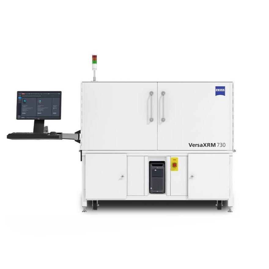

ZEISS Versa XRM X-ray Microscope
Image buried defects and package structures non-destructively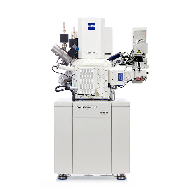

ZEISS Crossbeam laser FIB-SEM
Rapidly access site-specific features buried deeply within IC packages

ZEISS Crossbeam FIB-SEM
Achieve versatile, efficient imaging and processing for high-resolution 2D and 3D insights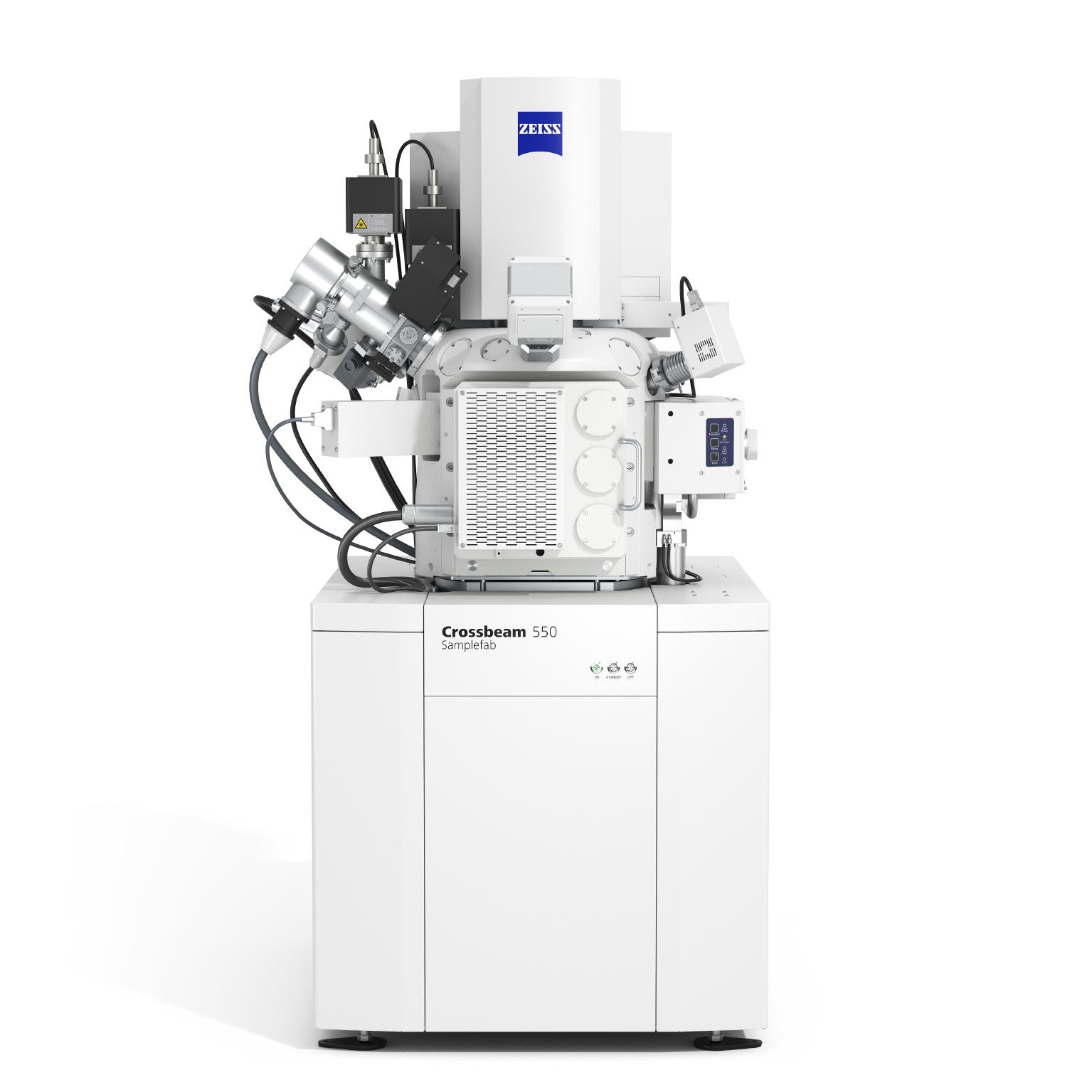

ZEISS Crossbeam Samplefab
Simplify sample preparation with fully-automated TEM lamella prep workflow
