Advanced nanofabrication shaping future technology in healthcare, electronics, and sustainability
At the National Graphene Institute (NGI) at the University of Manchester, UK, researchers are advancing nanoscience through e-beam lithography (EBL).
In NGI’s cleanrooms, scientists fabricate 2D material-based devices for applications in nano-fluidics, photonics, and quantum technologies – powered by ZEISS Scanning Electron Microscopes (SEMs) and RAITH ELPHY pattern generators.
A key success factor is close collaboration between research teams and technical support. Prof. Radha Boya, Professor of Nanoscience, and Dr. Lee Hague, Senior Technical Specialist, not only give insights into their collaboration. They share how advanced nanofabrication tools and expertise empower world-class research and inspire the next generation of scientists.
Advanced Functional Materials
Slit-shaped 2D channels:
A) Schematic diagram showing the cross-sectional view of the 2D slit-channels formed by sandwiching three layers, namely, top, spacers, and bottom layers. Cross-sectional SEM image of the channels of h
B) 8.4 nm
C) 60 nm
Advanced Functional Materials
Slit-shaped 2D channels:
A) Schematic diagram showing the cross-sectional view of the 2D slit-channels formed by sandwiching three layers, namely, top, spacers, and bottom layers. Cross-sectional SEM image of the channels of h
B) 8.4 nm
C) 60 nm
Research focus: precision nanostructures for 2D devices
NGI’s research focuses on fabricating nanoscale devices using materials like graphene. These devices feature ultra-fine structures – often below 100 nanometers – with tight spacing and complex geometries. Applications include nano-channels, waveguides, and quantum components requiring accurate multi-layer alignment. Achieving this level of detail requires tools that combine high-resolution patterning with flexible, repeatable workflows.
This work takes place in a multi-user, multidisciplinary environment. To meet varied fabrication needs, NGI relies on a flexible and high-performance nanofabrication setup – enabled by the integration of ZEISS SEMs and RAITH ELPHY systems – for consistent, scalable, and high-resolution results.
Prof. Boya’s group investigates angstrom-scale fluidic channels – atomically precise spaces only a few layers of atoms thick. These structures allow researchers to study how water, ions, and molecules behave under extreme confinement, uncovering new physical phenomena that don’t exist at larger scales.
Her team uses a top-down lithographic approach to fabricate these capillaries with ultra-smooth walls, enabling precise tuning of channel dimensions. This has implications for ion selective separations, selective gas and water flows, and ionic memory devices.
Recent work includes the fabrication of 2D slit-channels by sandwiching patterned MoS₂ layers, etched with PMMA masks, and sliced via ultramicrotomy for SEM imaging. These channels can be tuned from sub-nanometer to tens of nanometers in height, offering a versatile platform for studying molecular transport.
Technology in use: reliable tools for advanced nanofabrication
ZEISS SEMs and RAITH ELPHY pattern generators form one backbone of NGI’s daily workflows. Researchers use them to pattern and verify nanoscale structures such as etch masks for nano-channels, enabling repeatable fabrication of high-quality 2D devices.
ZEISS Sigma and EVO SEMs provide high-resolution imaging – even at low kV – while RAITH ELPHY supports both EBL and IBL (ion beam lithography). This integration allows seamless switching between small-feature and large-area exposures.
The ZEISS/RAITH solution is easy to teach to PhD students and post-docs. It provides a very accessible way to achieve great lithography results and allows the fabrication of high-quality 2D material-based devices.
Prof. Boya emphasizes that high-resolution imaging and nanofabrication are central to her research on angstrom-scale capillaries. Using the ZEISS SmartSEM software solution together with the Raith ELPHY Quantum NANOSUITE, her team can directly write complex patterns with exceptional precision. This reproducibility is essential when fabricating channels only a few atoms thick, where even the smallest variation could compromise results.
According to Prof. Boya, such accuracy is what makes it possible to investigate confinement-driven ion transport and push forward the boundaries of nanofluidics research.
In NGI’s cleanroom environment, intuitive software and stable optics ensure fast onboarding and reliable performance across projects. These tools have become essential for prototyping, iterative design, and pushing the boundaries of nanoscale engineering.
Seeing is believing. Microscopy lets us actually see what we’ve made. That’s invaluable at the nanoscale, where most things are invisible. It inspires students and gives them confidence to design their own experiments.
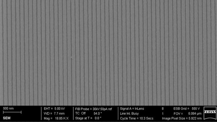
Nanofabrication of graphene channels for nano-fluidics
Ankit Bhardwaj
Etched few-layer graphene channels with ~40 nm width.
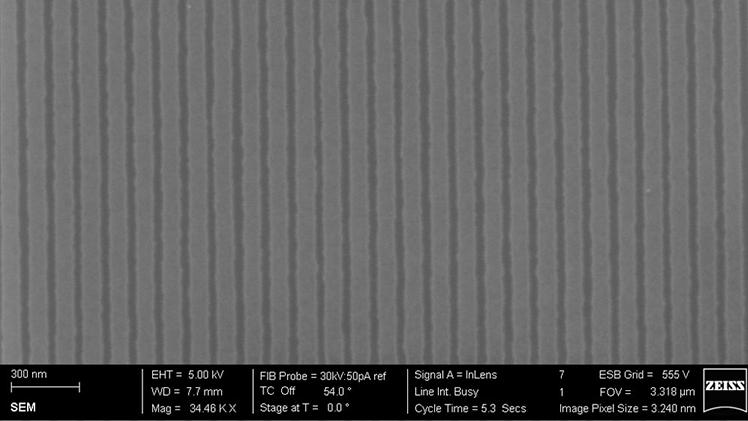
Ankit Bhardwaj
Etched few-layer graphene channels with ~ 40 nm width.
Dr. Lee Hague, expert in EBL systems, ensuring precision and performance in the cleanroom.
Expert support: driving research outcomes
Dr. Lee Hague oversees maintenance, training, and support for the ZEISS/RAITH systems. With over a decade of EBL experience, he helps researchers overcome fabrication challenges – especially in high-resolution, tightly spaced designs for nano-fluidics and photonics.
His role as trainer and system expert ensures consistent performance and knowledge transfer across generations of NGI researchers.
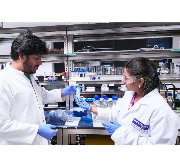
Prof. Radha Boya and her postdoc Dr. Hiran Jyothilal working on angstrofluidic devices to study water confined to one monolayer.
Expert Support: Driving Research Outcomes
Prof. Boya integrates microscopy into doctoral training programs and outreach activities. Her PhD students and postdocs gain hands-on experience with SEM and EBL, learning not just theory but also practice.
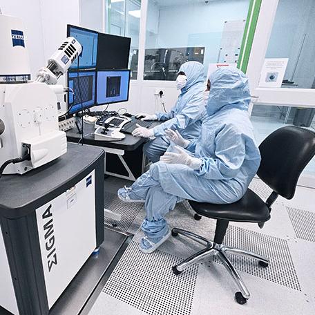
Prof. Radha Boya with her team member Dr. Hiran Jyothilal performing electron beam lithography (EBL) on a ZEISS Sigma system in a NGI cleanroom.
Expert Support: Driving Research Outcomes
She also shares microscopy images of graphene nanochannels in public lectures, school visits, and lab tours, sparking curiosity in younger generations.
My help and advice has helped many students to overcome fabrication challenges and increase the quality of their devices.
Technology partnership: ZEISS and RAITH integration
The collaboration between ZEISS and RAITH delivers a unified platform for imaging and lithography. This integration enables precise patterning and nanoscale analysis in a single workflow.
Adaptable across applications like nano-channel structures and quantum devices, the system’s reliability and usability are essential in NGI’s multi-user environment. Together, ZEISS and RAITH provide a flexible solution for advanced nanofabrication.
About the National Graphene Institute
The National Graphene Institute (NGI) at the University of Manchester, UK, is a leading research facility focused on graphene and other two-dimensional (2D) materials.
NGI provides 1,500 m2 of ISO Class 5 and 6 cleanroom space, supporting contamination-free fabrication and imaging workflows essential for nanoscale research.Its microscopy and imaging capabilities include scanning electron microscopy (SEM), focused ion beam (FIB), and light microscopy, used to analyze surface morphology, flake dimensions, and layer thicknesses of graphene-based structures.
Researchers at NGI also perform cross-sectional imaging of 2D heterostructures to study buried interfaces and atomic-scale features. These tools and environments support a wide range of applications, including nanoelectronics, photonics, quantum technologies, and nano-fluidics, making NGI a central hub for multidisciplinary nanofabrication and characterization.
To achieve ultra-fine structures below 100 nm – like nano-channels or quantum components – researchers use electron beam lithography (EBL) with systems such as ZEISS scanning electron microscopes and RAITH ELPHY pattern generators. These tools offer high-resolution patterning and repeatable workflows, even in multi-user cleanroom environments.
Reliable imaging and patterning tools are key. A setup combining ZEISS/RAITH instruments enables precise etch mask creation and verification, even for tightly spaced designs. Its intuitive software and stable optics make it easy to train new users and maintain consistent quality across projects.
In multidisciplinary labs, researchers often use setups that combine scanning electron microscopes (SEMs) with electron beam lithography (EBL) systems.
For example, pairing ZEISS Sigma or EVO SEMs with RAITH ELPHY pattern generators allows users to switch between small-feature and large-area exposures. These systems are known for their ease of use, making them suitable for labs where students, post-docs, and technical staff share equipment and collaborate on complex designs.