

ZEISS Materials Science Solutions Hub
Explore our solutions for your tasks and applications empowered by our electron and X-ray microscopesSolutions for Your Microscopy Needs
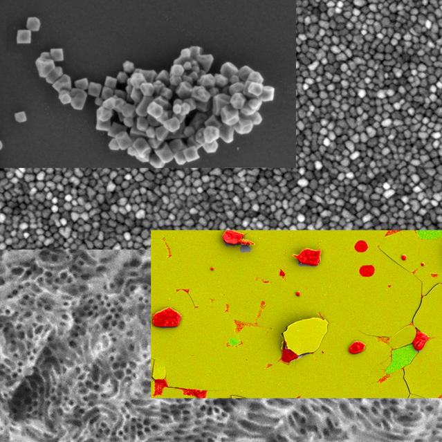
As a leading manufacturer of microscopes, ZEISS offers inspiring solutions and services for your materials research routines. Reliable ZEISS systems are used for manufacturing and assembly in high tech industries as well as exploration and processing materials worldwide.
Choose the ideal solution for your research by exploring the application areas below
Explore our Solutions for 3D X-ray Applications
Short description of the moduleXRM State of the Science Mini Series
High resolution X-ray microscopy (XRM) has grown out of the synchrotron community, to provide a critical capability in today’s suite of lab-based characterization equipment. As the field continues to evolve rapidly and new innovations expand the reach of the technique, tune in to this mini-series to gain quick updates on how XRM is making an impact in your field of work.


Voices in XRM
From students to post-docs, to professors and research scientists, X-ray microscopy is transforming the way people see and understand 3D morphology at the microscopic scale.
Enjoy the videos below extracted from our recent programs 3D in 3 Minutes and TomographyTuesday. Learn how scientists in diverse fields are using XRM to make innovative new discoveries.
Going 3D
A 4-part series to explore the scientific opportunities and increasing adoption of high resolution 3D X-ray microscopy within multi-user shared-instrument research facilities.
Explore our solutions for Electron Microscopy Applications
Short description of the moduleInnovators in EM
Innovators with different backgrounds discuss how their users and their organization have benefitted from owning a ZEISS field-emission scanning electron microscope. Each innovator has a unique amount of ZEISS SEM imaging and analytics experience and each one has improved the quality of their research by using our Gemini technology. Explore the success of FE-SEM owners and users from different backgrounds and experience.

FESEM Webinars
This multi-part workshop series provides insights into new discoveries in materials research. It is virtual and accessible from anywhere. This is part of our commitment to bring our expertise and application laboratory to you in an environmentally sustainable way.
Register for the series or watch our previous workshops relevant to your research.
Explore our Solutions for Semiconductor and Electronics Applications
Short description of the moduleXRM Packaging
Improve success rates & efficiency for semiconductor package failure analysis by using ZEISS 3D XRM technique to visualize your defect without altering it
Electronic Device and Materials
Transform your semiconductor sample prep and site-specific analysis by employing new and advanced microscopy techniques.
Parallel advances in FIB-SEM and 3D X-ray microscopy have radically changed sample preparation, characterization and failure analysis of semiconductor devices and packages. Learn how these techniques can help you high quality 3D images at high speed, find hidden defects, speed up sample prep and provide greater insights into semiconductor research, development and failure analysis
X-ray and FIB Particle Analysis
Accurately identify and analyze micron-sized defects buried within millimeter volumes of material. Learn how we characterized two isolated particles buried within a small iron plate and understand how you can apply this workflow to a variety of applications from life science to semiconductors..