Semiconductor technology is paving the way to a networked future
Dr. Christoph Zaczek has been involved in the development of more powerful microchips since the beginning of his career – always in close collaboration with dedicated teams at ZEISS. Sophia Tran is known as a tech influencer, among other things. As a user, the work carried out by Christoph Zaczek and his team is beneficial to her. But what does the development of microchips that are becoming more and more powerful actually mean for technological progress? The two of them met for a chat – about the future of the industry and our society.
The key player of the day is not much bigger than a fingernail. And when Dr. Christoph Zaczek holds it up to the camera, the camera has to zoom in: we're talking about a microchip. And the one Christoph Zaczek is holding in his hand is by no means the smallest. The world's smallest microchip measures just a few millimetres and has tiny nanometre-scale structures on its surface. As a comparison: one millimetre is a million times longer than one nanometre.
The structures of a processor are becoming smaller and smaller even though they are becoming more and more powerful. This is thanks to people like Dr. Christoph Zaczek. The 57-year-old is Fellow & Head of Architecture Process Development Optics at ZEISS Semiconductor Manufacturing Technology. He has dedicated his entire professional career to optical lithography – working on a process for chip production that can be used to manufacture ever more efficient semiconductors.
Conversation about innovations in semiconductor technology
Sophia Tran benefits from this. Among other things, she is a tech influencer and advises and invests in companies. If Zaczek is on the side of the developers, she is primarily on the side of the users and therefore brings the opposite perspective.
The two will now meet for the first time in Stuttgart. They talk about lithography, technology and artificial intelligence (AI), among other things. In short: about the future. But it is also about major social issues and the role that digital transformation plays in responding to them. And they keep coming back to talk about the small object in Zaczek's hand, which the camera can only capture when zoomed in and without which it would not even work: the microchip.
But what roles do semiconductors and their transistors play in our lives? How are they actually made? Where do they have a specific influence on society? And how are they changing the future?
Semiconductors have brought people closer together over the past decades. And AI will take this to a whole new level.
Third-party Content Blocked
The video player is blocked due to your cookie preferences. To change the settings and play the video, please click the button below and consent to use of "Functional" tracking technologies.
Growing demand for more processing power
Some microchips are only a few millimeters in size – and yet they are everywhere. "They are in pretty much every electrical household appliance," says Zaczek – in vacuum cleaners, in dishwashers and in coffee machines. Devices such as smartphones, computers or tablets would not work without these small microprocessors. And technological innovations such as automation, AI or autonomous driving would be inconceivable without them.
So the world is need of more and more processing power. The chip industry has to supply them. And they have already been doing so for decades. Gordon Moore once wrote that the number of transistors per area on a wafer – and therefore the processing power of the chip – doubles approximately every two years. This was in 1965 and went down in history as Moore's Law. At the time, the engineer and entrepreneur would never have thought it possible that this would still be the case. Yet ZEISS, and especially its strategic partner ASML, have made it possible thanks to their solutions.
Over time, the Dutch high-tech company ASML has developed from being a niche supplier on the European market into a global industry leader in the field of semiconductor technology and is now the sole manufacturer of EUV lithography machines. EUV stands for "extreme ultraviolet". EUV lithography was implemented by ASML along with ZEISS and many other partners from Europe and the US. This development has decisively changed people's digital lives and work.
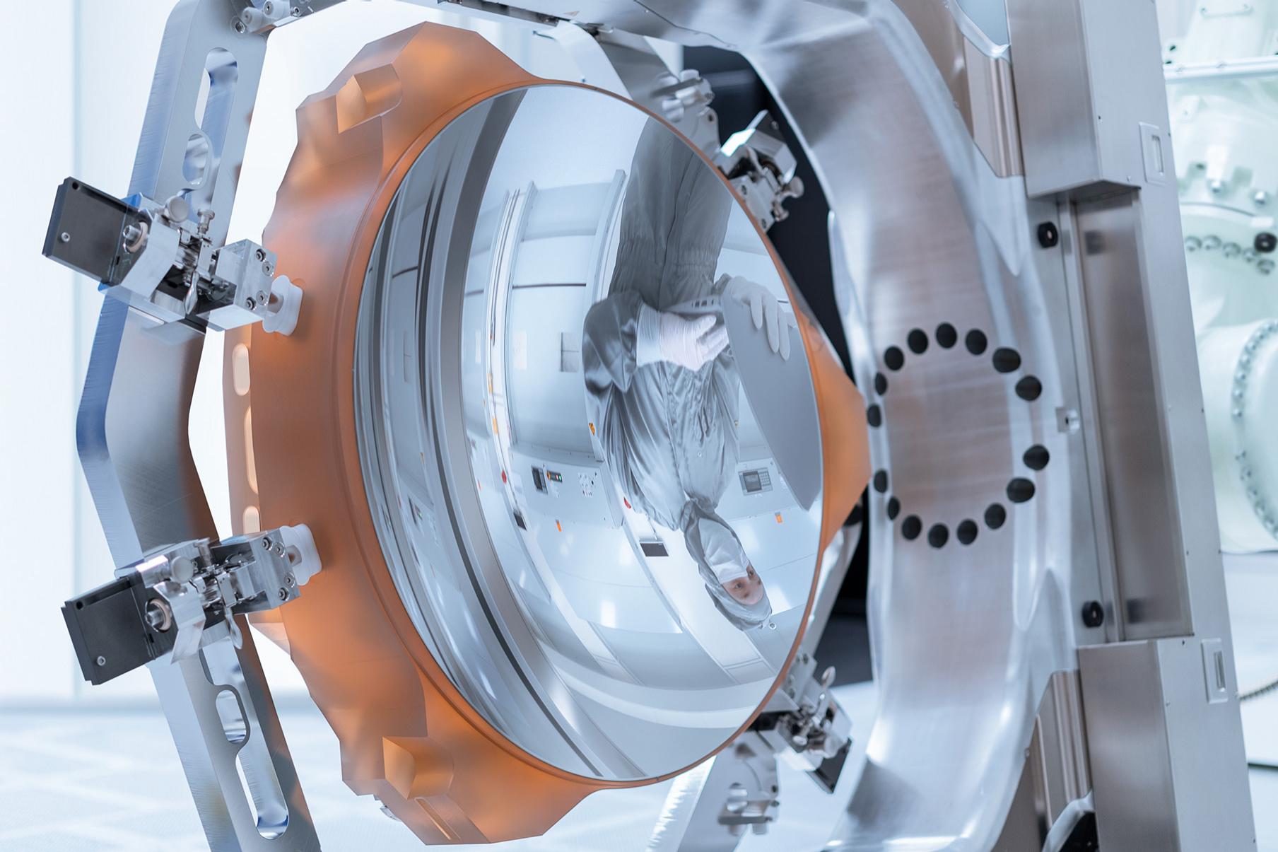
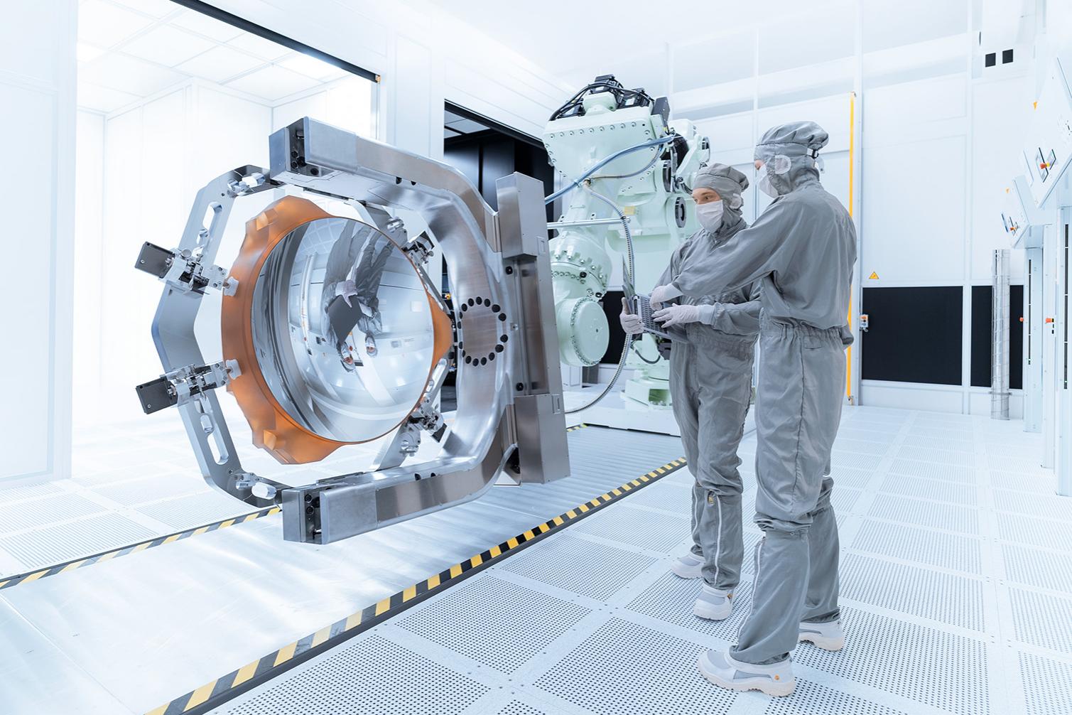
Christoph Zazcek explains, "At ZEISS, we are very proud to be an important part of this widely connected and highly innovative ecosystem and to tell our story as part of the EUV story. Our optics can be described as the most precise mirrors with mechatronic systems and they are at the heart of the EUV systems of our strategic partner ASML."
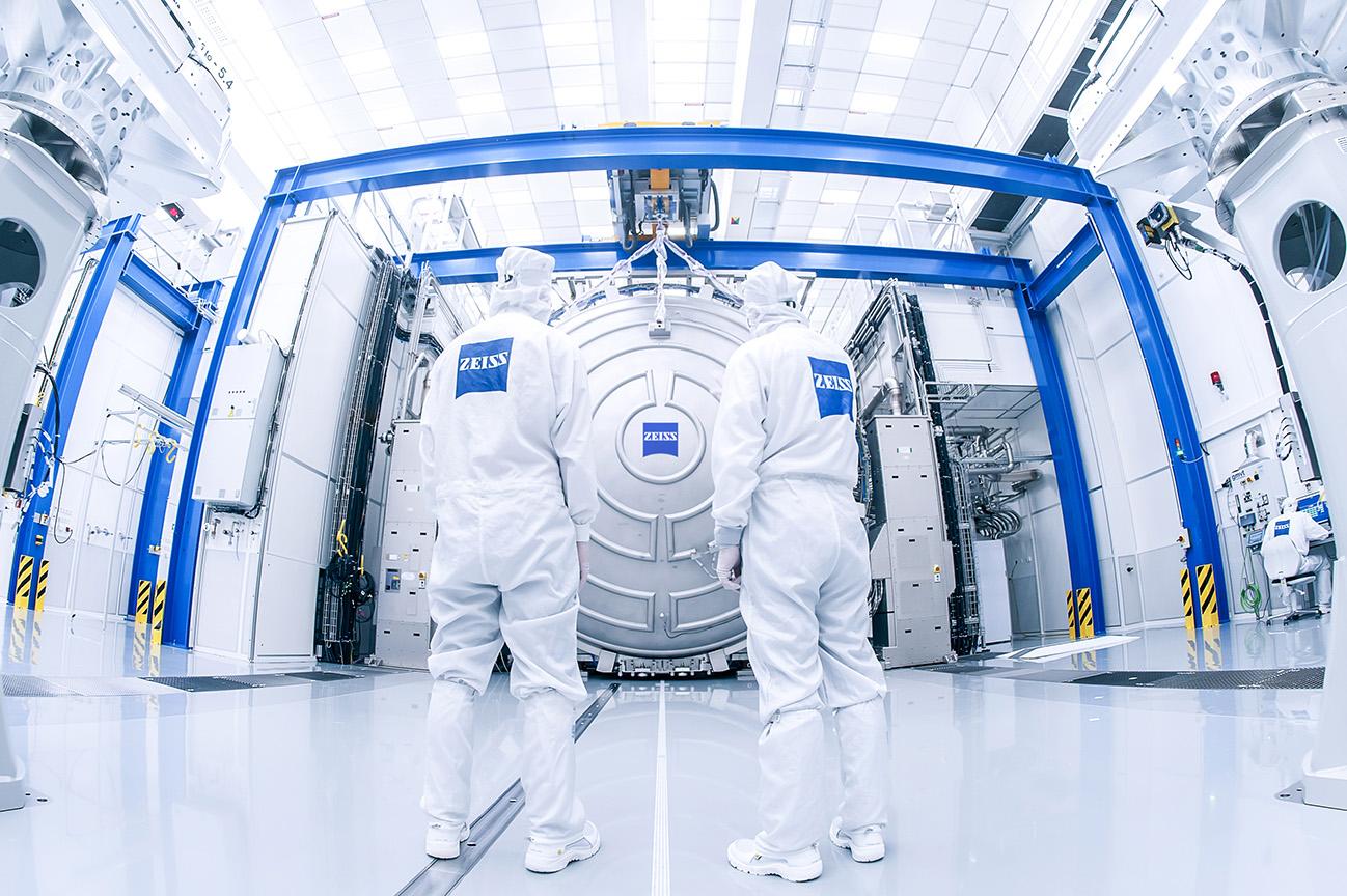
Semiconductor technology at ZEISS
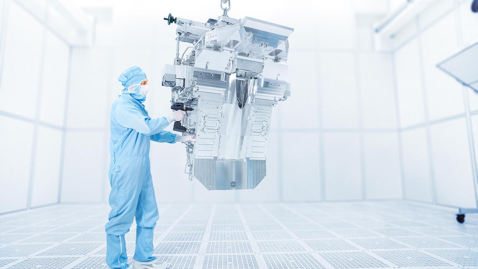
ZEISS Semiconductor Manufacturing Technology (SMT) has been shaping semiconductor technology for more than 50 years. 80 percent of all microchips worldwide are manufactured with optics from ZEISS and the lithography systems of its strategic partner ASML. Optics from ZEISS SMT are at the heart of chip production. Using ever shorter wavelengths, it has been possible to project ever finer structures onto the wafer. DUV technology ("deep ultraviolet light") with wavelengths of up to 193 nanometers was the first milestone in production. EUV lithography currently achieves wavelengths of up to 13.5 nanometers. This is smaller than a virus. The next development step is imminent: high-NA-EUV lithography is set to go into series production in 2026. "High-NA" stands for high numerical aperture. It describes the angular range from which an optical system can pick up light. The greater the angle, the finer the details are that are displayed. In the case of high-NA EUV lithography, it's 0.55. By comparison, the current EUV lithography is 0.33.
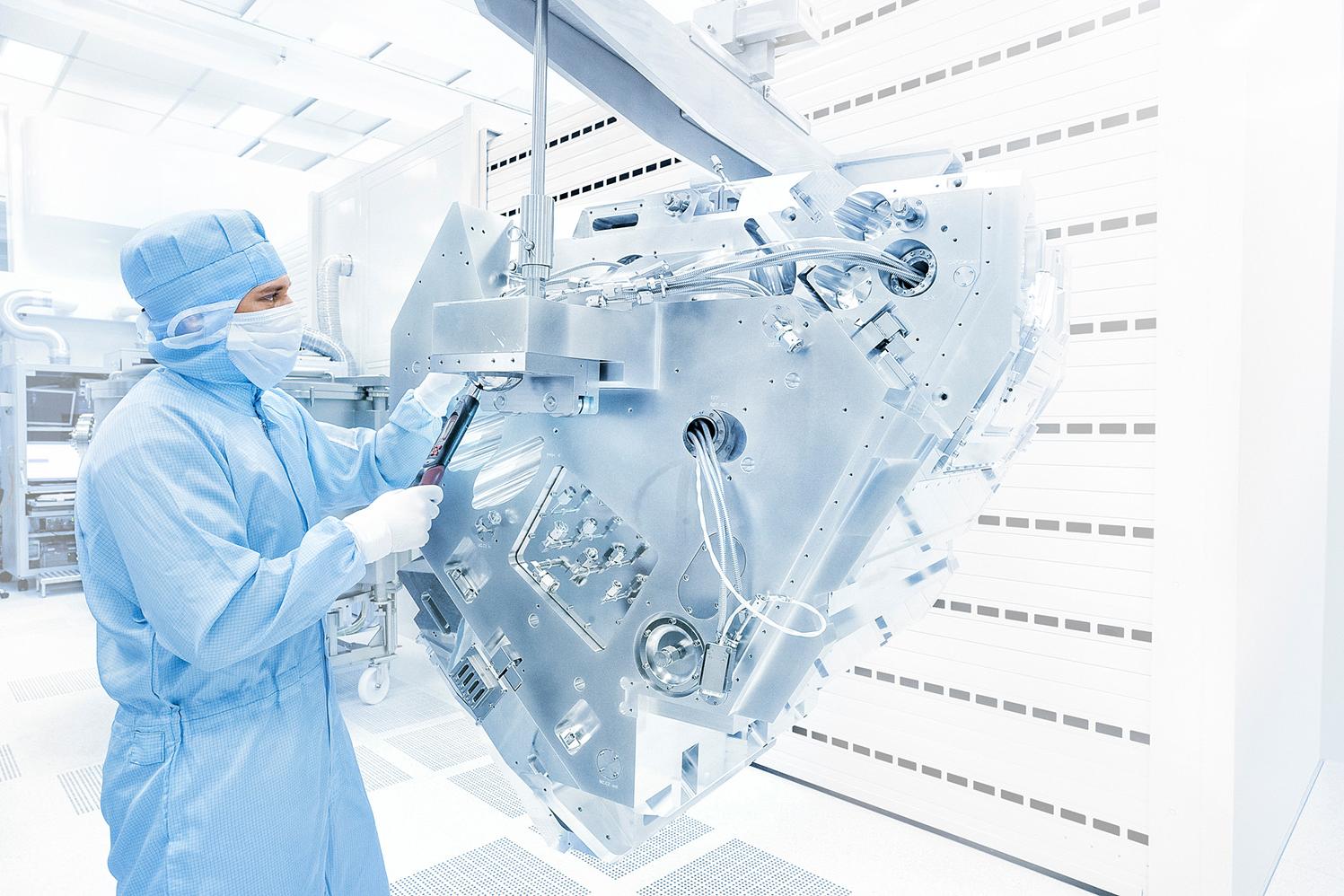
Optical lithography: the heart of chip production
The mirror used for the heart of the latest EUV generations has a diameter of over one meter and weighs several hundred kilograms. It is also polished so smoothly that the largest unevenness is smaller than an atom. If the mirror were Germany, the highest peak or "Zugspitze", would not be 2,962 meters high, but only a tenth of a millimeter. The sensors and actuators of the projection optics work so precisely that a reflected laser could hit a golf ball on the moon.
Such orders of magnitude in production create the computing power that makes innovations such as AI possible in the first place. Especially if these technologies are to be accessible and usable for everyone, as is already the case with AI. In this sense, microchips are paving the way for AI, which is currently changing the world. But what opportunities does this open up? "It's difficult to predict," says Christoph Zaczek, "but at least it's already foreseeable." He cites autonomous driving as an example, "I told my car this morning where I wanted to go – and it navigated me to Stuttgart. It won't be long before it will be driving me to my destination in Germany on its own. This is already possible in some places in the world."
More closely connected world
More and more processing power means that the amount of data can be processed faster and better. This is the case with mobility – and with many other areas of life, such as healthcare, the world of work in general, but also in our personal life and therefore the everyday lives of many people.
For this reason alone, technological progress with the emergence of ever more efficient microchips has an effect on society, observes Sophia Tran and believes: "Our coexistence will change fundamentally during the digital age. Technology is both the basis and the driver for this. And microchips are the core element for this."
Dr. Christoph Zaczek shares this opinion. He says: "Semiconductors have brought people closer together over the past few decades. And AI will take this to a new level." What does he mean by that? For example, when it comes to knowledge management, AI is ideally suited to making knowledge available globally and appropriately. For example, language barriers can be easily broken down with real-time translations using AI.
How we live together will change fundamentally during the digital age. Technology is both the basis and the driver for this. And microchips are the core element for this.
The next major steps are already on the horizon: photonic circuits in chip assembly can increase performance while simultaneously reducing energy requirements. "This is also important in terms of sustainability," says the 57-year-old. After all, a lot of processing power has so far also required a huge amount of energy.
In order to keep up with the pace, ZEISS is taking a systematic approach to development. "We are already thinking about products that could be relevant in ten or 20 years' time. This long-term approach is made possible by the ZEISS foundation concept," explains Christoph Zaczek. This also means that ZEISScan invest around 15 percent of its turnover in research and development. In terms of implementation, he refers to this as roadmapping: "We observe the dynamic semiconductor market, talk to customers and our strategic partners and evaluate their requirements. We derive our product roadmaps from this," says the scientist.
One of these roadmaps describes the need for an additional, classic reduction in the size of the structure. In other words, microchips need to continue to become smaller – and at the same time even more powerful. Semiconductors are currently still produced using DUV and EUV lithography. However, the next development step is already imminent: high-NA-EUV lithography is set to go into series production in 2026. The right process for the next stage after that has also already been found: hyper-NA-EUV. However, it is currently still being developed. According to the expert, this will take around 10 to 15 years. He will therefore continue to be involved in shaping the future.
Sophia Tran
Influencer, founder, presenter, investor: Sophia Tran is many things, but, more than anything, she is passionate about technology. She studied electrical engineering at RWTH Aachen University and business administration for her Master's degree. Her professional background includes the management consultancy Detecon International (Deutsche Telekom), the luxury group LVMH and a business publishing house. She also helped build up the incubator and accelerator DIGITALHUB.de as an authorized signatory. In 2021, she finally founded the company Spotlight! Ventures, her own consulting agency for start-ups.
Dr. Christoph Zaczek
Dr. Christoph Zaczek has dedicated his entire professional career to optical lithography. He studied physics in Stuttgart, Ulm and in Portland, and has been publishing scientific papers on the subject of optical lithography since the late 1990s. He started working at ZEISS as a doctoral student in 1998, and is still there today. Zaczek joined ZEISS Semiconductor Manufacturing Technology as a senior scientist in 2001. Today, he is Fellow & Head of Architecture Process Development Optics.
In focus: Semiconductor technology in transition
Microchips are the driving force behind the digital transformation because they form the technological basis for innovations in almost all areas of the modern world. They provide the necessary processing power for computers, smartphones and servers, enabling complex tasks to be completed efficiently. Microchips are also a crucial component for networking devices in the Internet of Things (IoT), enabling automation and intelligent control. Advances in chip technology are also resulting in more energy-efficient devices, which is particularly important for more innovative technologies and sustainable IT infrastructures. The miniaturization of microchips allows manufacturers to develop more compact and portable devices such as wearables. In addition, microchips support the performance of artificial intelligence (AI) and machine learning (ML), enabling new applications in integrated areas such as speech recognition, image processing and autonomous driving.
Progress in the production of microchips depends substantially on optics which are at the heart of the lithography systems. The key factor here is the wavelength of the light with which the structures are projected onto the wafers. Semiconductors are currently produced using DUV and EUV lithography. in the case of EUV, the wavelength of the light is 13.5 nanometers. This makes the structures on the chip around 5,000 times finer than a human hair. The next stage has been achieved with high-NA-EUV lithography. The difference compared to EUV lithography is the size of the numerical aperture. It describes the angular range from which an optical system can pick up light. The greater the angle, the finer the details are that are displayed. In the case of high-NA EUV lithography, it's is 0.55. By comparison, the current EUV lithography is 0.33. The next generation is set to go into series production in 2026.
The semiconductor industry plays a crucial role in overcoming global challenges such as digital transformation and the integration of artificial intelligence (AI). It develops more powerful and efficient chips that form the backbone of modern digital systems. Specialized AI processors accelerate applications and enable the broad integration of AI technologies. Microchips are essential for the Internet of Things, which promotes intelligent and automated systems in a wide range of areas. The industry is also continuously improving the energy efficiency of chips, which helps to reduce energy consumption. Advances in semiconductor technology also support new technologies such as 5G and autonomous driving. Thanks to its scalability and adaptability, the industry enables a rapid response to technological changes and supports global adaptation to the digital landscape and the associated demand.