Micro- and Nanofluidics
Precise Nanopatterning and Charge-Free, Non-Destructive Imaging of Future Nanofluidic DevicesNanofluidic devices can help you study fundamental scientific processes and probe a variety of mechanisms like nanocapillarity, mass transport in confined structures, and DNA-protein interactions.
One advantage of nanofluidic devices for these studies is their flexibility when it comes to size and shape. These features can be engineered with precision using electron and ion beams, allowing scientists to tune various properties as required. But in order to fabricate nanofluidic devices with the precision needed for future applications, standard FIB-SEM tools are far from ideal.
Standard Tools Are Not Sufficient
For instance, charging of insulating samples in an SEM is a big problem because it distorts the image. One solution to this is depositing a conducting metal on the surface of the sample to be studied. But this damages the sample and makes it unusable afterwards. On the other hand, charge neutralization in an SEM means you can image nanofluidic specimens non-destructively, and without coating them with a metal thin film.
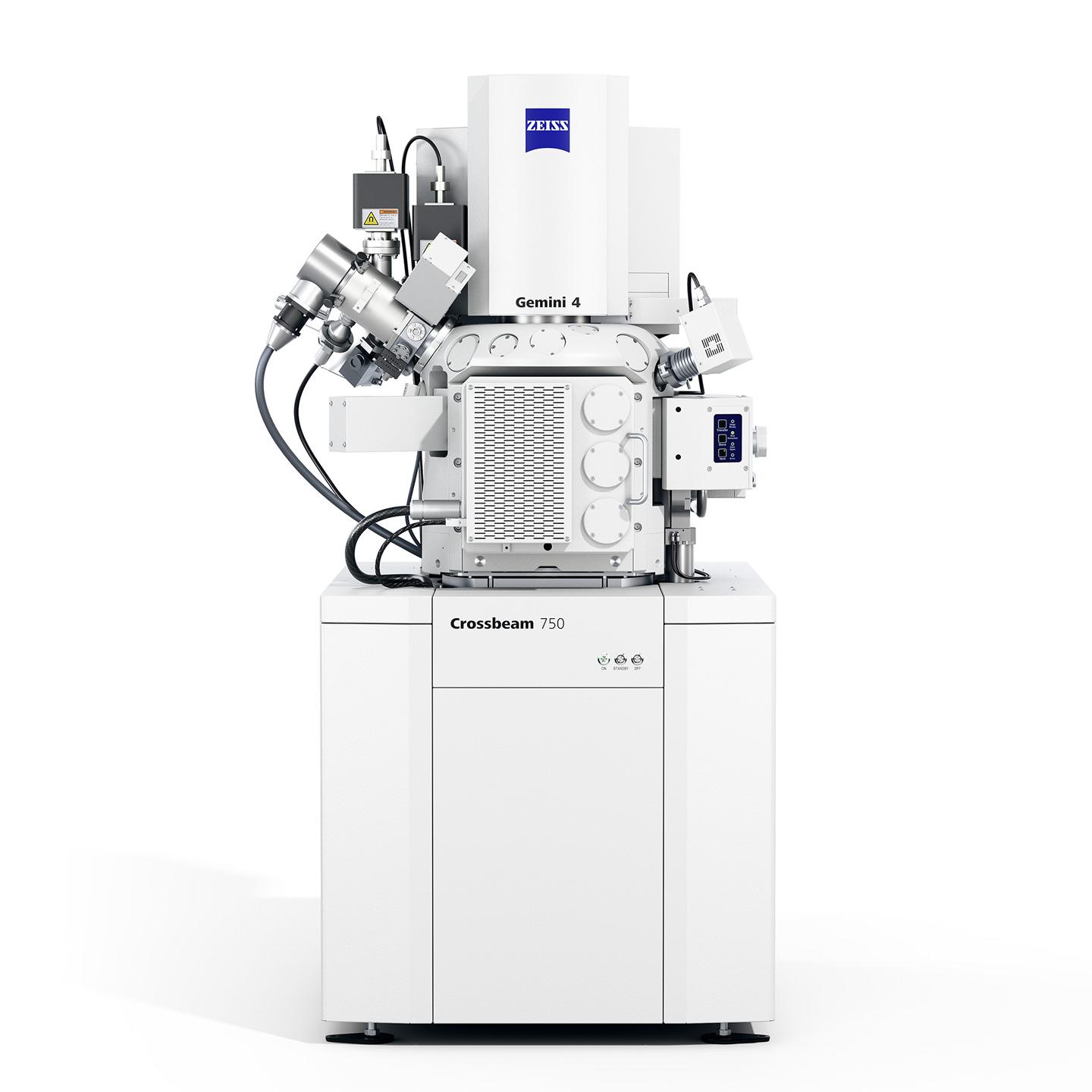
Traditional FIB-SEM instruments are no longer sufficient for today’s nanomaterials research. When it comes to pushing nanofluidics further, the ability to combine outstanding SEM imaging performance with high FIB sample throughput is critical. Also important is the ability to upgrade your FIB-SEM in a modular fashion as your needs grow. With this kind of modular platform concept, your microscope can keep up with your increasing research demands.
You Need the Right Tools for Your Research
Bottom line: the tools you use must keep pace with the demand. To this end, ZEISS is committed to helping scientists push nanofluidic research forward. You are offered damage-free, high-performance SEM imaging at low kV, combined with high FIB sample throughput and massive material ablation capabilities.
Application Examples