FIB-SEM for Electronics & Semiconductors

Failure analysis and 3D device characterization

Support physical failure analysis, technology pathfinding, and process yield control in semiconductor and electronic device applications.

ZEISS Crossbeam FIB-SEM provides precise cross-sectioning, TEM lamella preparation, and 3D tomography for semiconductor workflows. Real-time imaging combined with integrated analytics enables access to buried structures and produces reliable, high-resolution results.

Accelerate electronics development with confidence

As electronic devices continue to scale, semiconductor teams need rapid access to buried structures and precise, repeatable preparation to reduce variability. ZEISS Crossbeam integrates high-resolution Gemini SEM imaging with precise FIB processing to unify milling, imaging, and analytics in a controlled 3D workflow. Real-time monitoring, automated TEM lamella preparation, and serial tomography improve endpoint accuracy and enable reliable reconstruction of complex device structures.

TEM lamella preparation for electronics workflows

ZEISS Crossbeam FIB-SEMs enables guided and automated TEM lamella preparation in ZEN core EM, integrating precise FIB processing with high-resolution SEM imaging for controlled thinning and targeted endpointing. This enables characterization of structural, chemical, and physical properties at the nanometer scale.
  • Automated, guided multi-site TEM lamella preparation

    Automated, guided multi-site TEM lamella preparation

  • Lamella chunk preparation

    Lamella chunk preparation

  • Lamella lift-out

  • Attach lamella to grid

    Attach lamella to grid

  • Lamella thinning and endpointing

  • Automated, guided multi-site TEM lamella preparation
  • Lamella chunk preparation
  • Lamella lift-out
  • Attach lamella to grid
  • Lamella thinning and endpointing
ZEN core EM user interface

What you can do with Crossbeam

  • Collect data in a timely manner with automated lamella preparation and thoroughly investigate precious samples while controlling the workflow manually.
  • Investigate diverse materials in a single run. Adapt FIB parameters for different materials and create a recipe library.
  • Run the entire workflow with a single user interface: ZEN core EM lets you perform each step of lamella preparation in a streamlined manner.

The Crossbeam portfolio

See while you mill, choose what fits

ZEISS Crossbeam at work

Guided-to-automated workflows with ZEN core EM

All ZEISS Crossbeam models support TEM lamella preparation via predefined ZEN core EM workflows, with structured steps for trenching, thinning, lift-out, and on-grid refinement to ensure consistent process control.

Workflow highlights

  • Batch execution for higher throughput with process lists, unattended runs, and mixed materials or settings in a single sequence.
  • Operator safeguards with safety checks, prompts, and pause/log/resume functionality to maintain preparation accuracy.
  • Rotational and angular nudging of the FIB scan pattern to refine alignment and improve endpoint precision.

"See while you mill" during thinning

Final polishing is critical for TEM lamella quality. Gemini field-free optics provide clear SEM imaging at preparation tilt, enabling real-time adjustment of key parameters:

  • Energy/current steps
  • Nudging
  • Scan strategy

HDR Mill + SEM with Crossbeam 750

ZEISS Crossbeam 750 integrates HDR Mill + SEM, interweaving simultaneous SEM and FIB scanning to maintain image clarity at higher beam currents without interrupting milling, accelerating coarse removal while preserving process visibility.

Fully automated high-volume TEM preparation

ZEISS Crossbeam Samplefab is a dedicated automation solution for high-volume TEM lamella production, standardizing bulk-to-grid preparation to ensure repeatability, traceability, and consistent lamella quality across operators, shifts, and production sites.

Crossbeam 750 HDR Mill+SEM imaging of a 5 nm SRAM structure (left) showing clear nanoscale detail during milling.
Crossbeam 750 HDR Mill+SEM imaging of a 5 nm SRAM structure (right) showing clear nanoscale detail during milling.

Targeted cross-sections and defect localization

Crossbeam synchronizes FIB milling with real-time SEM imaging, enabling continuous parameter adjustment and refined probe and detector control for improved defect localization. At higher beam currents, where secondary electron noise and signal aliasing increase, HDR Mill + SEM interweaves the signals to preserve image clarity without interrupting milling, supporting more consistent preparation of complex structures.

Key capability
Acquire high-resolution images of cross-sections to obtain sub-surface information. Crossbeam offers a wide range of detectors for a comprehensive characterization of your sample; up to four detector signals can be acquired simultaneously.

  • FIB tomography of a 5 nm SRAM device over a large area showing nanoscale structural detail across the sample.

    3D FIB-SEM tomography and analytics for device understanding

    FIB-SEM tomography on ZEISS Crossbeam performs serial cross-sectioning to image and reconstruct sample volumes in three dimensions. Intelligent software solutions enable extended, unattended tomography runs, delivering reliable, precise results efficiently.

  • 3D EDX maps acquired during FIB-SEM tomography

    3D EDX map and FIB tomography of a power MOSFET device, prepared with Crossbeam 550L, showing elemental distribution and nanoscale structure.

    3D analytics

    ZEISS Crossbeam supports 3D acquisition for R&D and failure analysis, enabling accurate reconstruction with integrated EBSD and EDS to correlate structural and compositional data in complex device structures.

  • XRM to FIB-SEM correlative workflow showing targeted transfer from X-ray microscopy to focused ion beam SEM analysis
    XRM to FIB-SEM correlative workflow showing targeted transfer from X-ray microscopy to focused ion beam SEM analysis

    XRM to FIB-SEM correlative workflow showing targeted transfer from X-ray microscopy to focused ion beam SEM analysis

    XRM to FIB-SEM correlative workflow showing targeted transfer from X-ray microscopy to focused ion beam SEM analysis

    Multi-scale correlation

    Atlas 5, ZEISS correlative imaging software, enables multi-scale, multi-modal workflows by correlating images and integrating X-ray volume data to target buried features and reduce the risk of missed regions of interest.

Hardware capabilities for semiconductor workflows

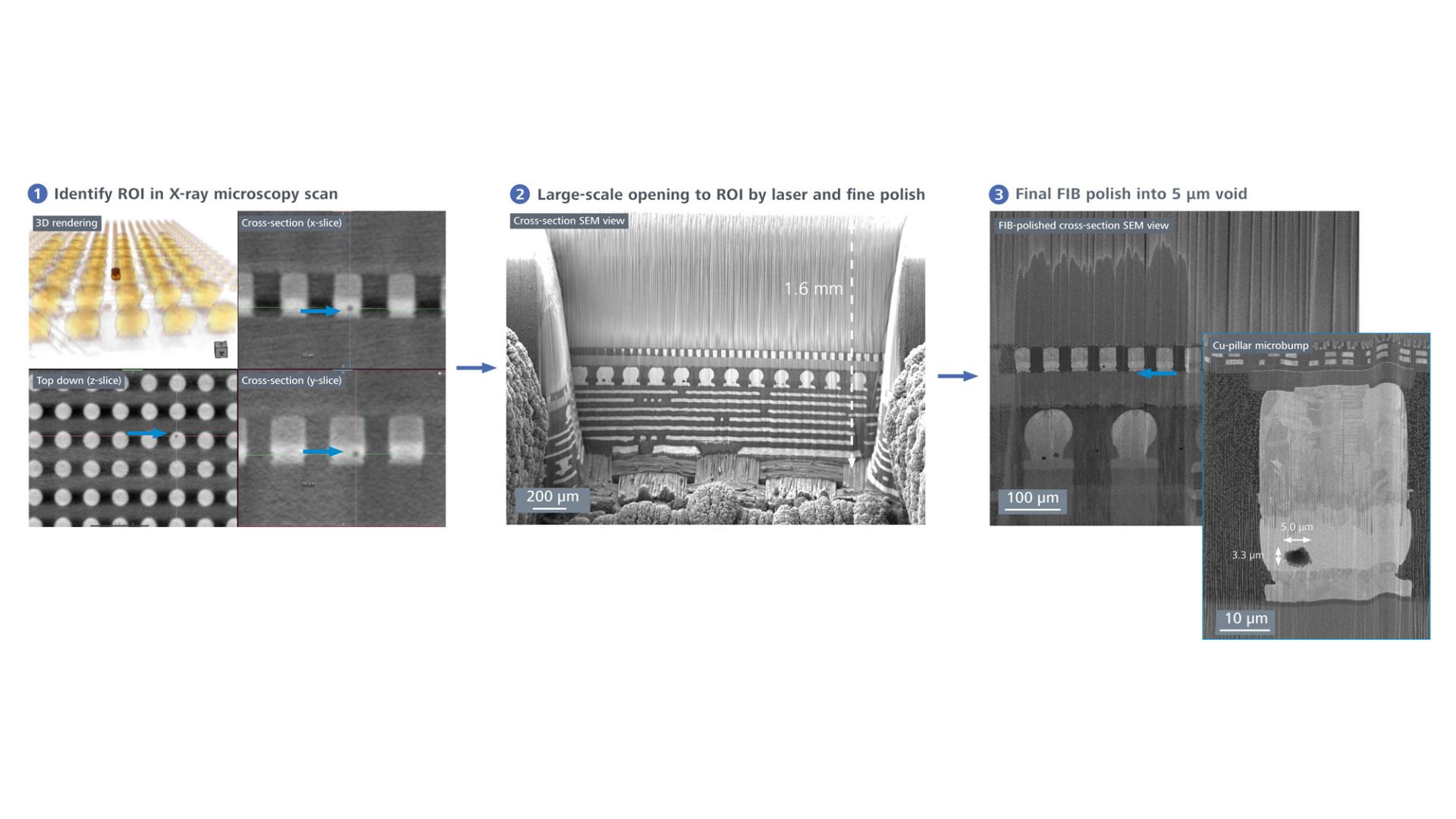
  • The femtosecond laser removes millimeter-scale volumes in minutes, increasing throughput and enabling rapid access to buried device features for XRM, APT pillars, and large-area TEM lamella preparation. It produces clean EBSD- and EDS-compatible cross-sections, with the FIB reserved for final polishing to reduce time and potential damage.

    What you can achieve

    • Access deeply buried structures quickly.
    • Prepare mm-scale cross-sections in width and depth.
    • Minimize damage and heat effects thanks to ultrashort laser pulses.
    • Locate hidden ROIs by correlating with X-ray microscopy datasets.
    • Automate the workflow tasks and seamlessly transfer to the FIB chamber.
  • ZEISS Crossbeam is available with two chamber sizes to expand analytical, imaging, and sample-modification capabilities. The large-chamber configuration supports processing large samples and full wafers up to 200 mm, enabling greater flexibility in semiconductor workflows.

    Highlights

    • 150 mm or 200 mm stages: standard or optional high-precision (HP) stage
    • 200 mm airlock with extension rails for smooth wafer transfer
    • NavCam raiser for full-wafer imaging and fast ROI navigation
    • Built-in safeguards to prevent wafer-chamber/column interference
    • Heavy-load transfer capability (>500 g) with robust rod/holder system
  • The FE-SEM column in Crossbeam uses Gemini electron optics with a field-free objective lens, preventing strong magnetic field exposure and enabling distortion-free, high-resolution imaging across large fields of view, even at tilt, while preserving sample integrity in sensitive semiconductor investigations.

    • Gemini 1: Available on Crossbeam 350, offers flexibility and supports Variable Pressure imaging for samples that exhibit charging or outgassing.
    • Gemini 2: Featured on Crossbeam 550, delivers high-resolution imaging at low kV, combined with the beam current required for demanding analytical and preparation workflows.
    • Gemini 4: Integrated into Crossbeam 750, significantly raise low kV resolution/SNR — even at tilt — while reducing objective lens field influence on the low energy FIB probe under high-resolution SEM conditions.

    Ion-sculptor FIB
    The Ion-sculptor FIB column spans 1 pA to 100 nA, enabling rapid bulk removal and controlled low-energy finishing within a single, scalable workflow.

Accessories and add-ons for electronics characterization

  • ToF-SIMS ion maps of a GaN device prepared with Crossbeam FIB-SEM, showing spatial distribution of aluminum, oxygen, nitrogen compounds, and titanium across the structure.

    ToF-SIMS

    Enables parallel detection of atomic and molecular ions down to the ppm level, including analysis of light elements such as lithium and isotopes.

  • STEM imaging modes (BF, DF, ADF, HAADF, ODF) of a GaN device cross-section using Crossbeam FIB-SEM, highlighting structural contrast and material interfaces.

    STEM

    Use a retractable scanning transmission electron microscopy (STEM) detector with segmented annular dark field (ADF) as well as high angle annular dark field (HAADF) to image thin samples directly in the FIB-SEM chamber for high-contrast nanoscale structural analysis, in-situ orientation/defect mapping and critical dimension (CD) metrology.

  • EDS elemental maps of a GaN device cross-section acquired with Crossbeam FIB-SEM, showing distribution of Al, O, Au, Ga, N, and Si across layered structures.

    EDS

    Integrate elemental analysis during cross-sectioning and 3D workflows with multi-detector acquisition for comprehensive material characterization.

Downloads

  • ZEISS Crossbeam 750

    Deliver first-time-right sample preparation for even the most challenging targets

    3 MB


Contact us

Explore Crossbeam in detail

Download the product brochure — get the specifications and technical insights you need.

Form is loading...

If you want to have more information on data processing at ZEISS, please refer to our data privacy and legal notice.

Dive deeper with the whitepaper

Access in-depth insights, practical workflows, and expert analysis.

Form is loading...

If you want to have more information on data processing at ZEISS, please refer to our data privacy and legal notice.


Share this page