ZEISS Intelligent Workflows

ZEISS @ Semicon Europa

Register for a free ticket
Starting soon
starting on
Ongoing Stay Tuned for next time
Ended Stay Tuned for next time
  • 00 years
  • 00 months
  • 00 days
  • 00 hours
  • 00 minutes
  • 00 seconds

Enabling Next-Generation Semiconductor Devices

ZEISS Solutions for Semiconductor Development, Manufacturing and Analysis

With the most comprehensive imaging portfolio in the industry, ZEISS delivers cutting-edge solutions across the entire semiconductor value chain—from wafer fab to packaging and assembly. For mask making and lithography, ZEISS enables zero defect strategies, in-die metrology, and precise overlay control. Its process control and failure analysis tools provide actionable insights to meet the challenges of next-gen semiconductor devices.

Register for a free trade show ticket and visit ZEISS at Semicon Europe. Semicon will be held in parallel to Electronica, the ticket is valid for both events.

Visit ZEISS also at Advanced Packaging Conference (APC) on Nov 11 and MEMS & Imaging Sensors Summit on Nov 12. Location: ICM Munich

Please note:

  • Online registration in advance is required.
  • The online voucher link can only be redeemed once and is valid for one person at a time.
  • Use the mobile ticket for smartphone and tablet or the Print@home-Ticket.
  • The ticket is valid for Semicon and Electronica during the trade fair times.
  • After registration you will receive a ticket code from ZEISS to register for the free ticket at Messe Munich. ZEISS will send the code in a separate email at a later time. Please check your spam or junk folder if necessary

💡 Meet us at our booth to experience

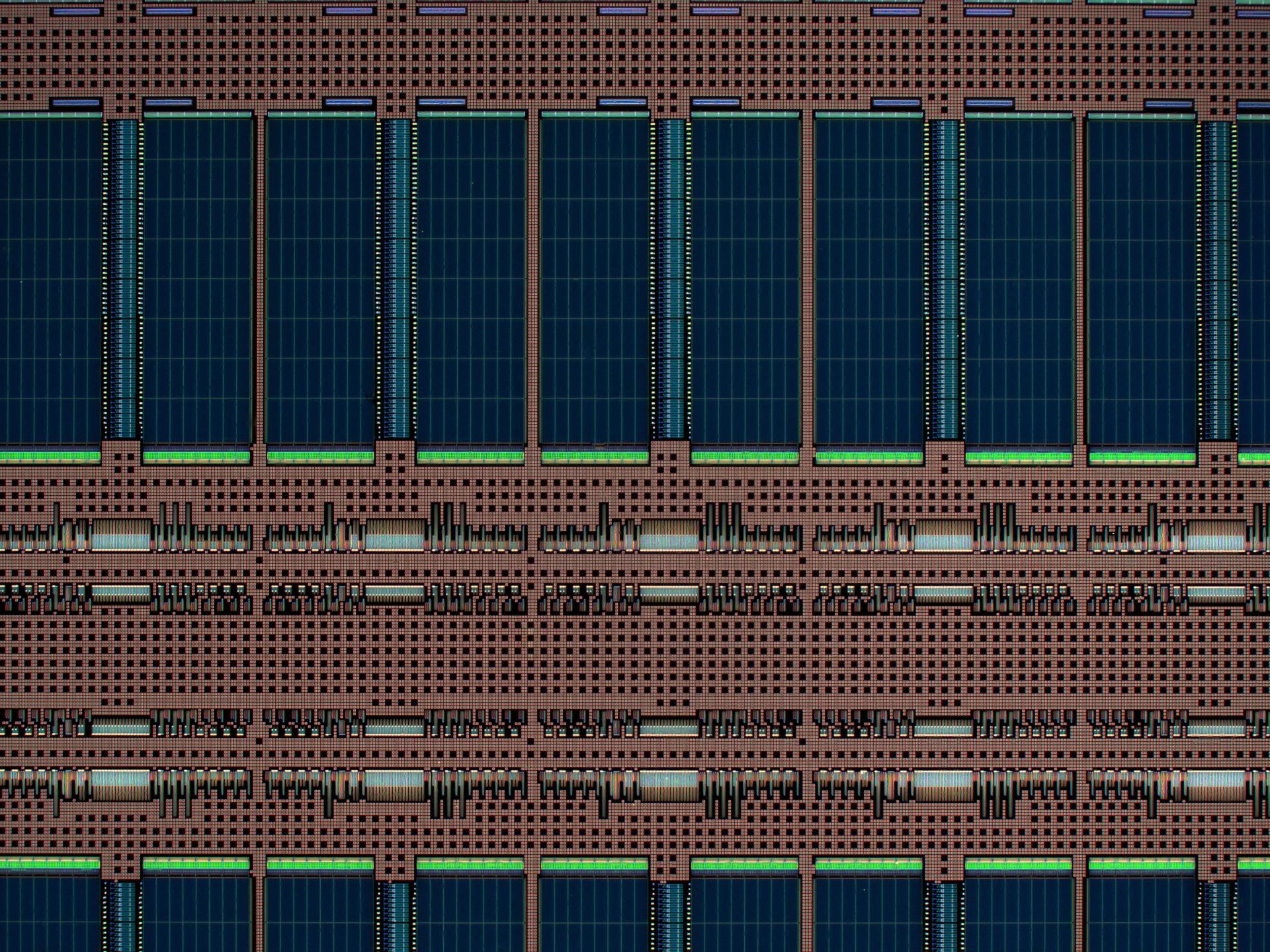
Multi-Site lamella preparation in silicon using ZEN TEM Prep module in ZEN core. The array contains 7x6 1µm thick lamellas, aka chunks.

Advanced FIB-SEM Analysis for Semiconductor Failure Investigation

Investigating defects and buried structures is essential for semiconductor failure analysis and process development. Explore critical interfaces, reveal subsurface defects, and examine complex device architectures using targeted material removal and high-resolution imaging with ZEISS Crossbeam Laser and Crossbeam 750.

Automated TEM Lamella Preparation

High-quality TEM samples are essential for analyzing nanoscale defects, thin films, transistor structures, and interfaces in semiconductor devices. ZEISS Crossbeam SampleFab supports automated lamella preparation, helping improve workflow efficiency and reproducibility for demanding semiconductor applications.

Non-Destructive Inspection and Advanced X-ray Microscopy

Reveal internal defects, voids, cracks, and structural anomalies in semiconductor devices and advanced packages without initially sectioning the sample. ZEISS Context CT, X-ray microscopy, NLX, and Xradia Ultra support three-dimensional characterization across different scales, from component inspection to nanoscale analysis using nanoCT and nanotomography.
Optical Microscopy and Connected Software Workflows

Optical microscopy enables rapid inspection, defect screening, and identification of regions requiring further investigation. Combined with ZEISS imaging and analysis software, it supports the correlation of information across optical, electron, and X-ray microscopy for a more comprehensive understanding of semiconductor materials and devices.
Location

Semicon

Semicon Munich Messe München, Hall B1 Booth 618 81829 Munich Germany

Registration

Form is loading...

If you want to have more information on data processing at ZEISS please refer to our data privacy notice