Advanced Analysis for Complex New Materials and Structures
Faster Time to Market with Accurate Failure AnalysisThe mobile communication, Internet of Things (IoT), cloud computing, and the electrification of automotive industries are driving huge demand for high-performing “More than Moore” semiconductor devices, which require the integration of new materials and processes, or novel silicon architectures and packaging technologies such as micro-electromechanical systems (MEMS). Direct band gap and wide band gap materials such as gallium arsenide (GaAs), silicon carbide (SiC), and gallium nitride (GaN) present new challenges to equipment manufacturers and device fabricators alike. Many of these devices also integrate traditional ICs, which creates fabrication and packaging challenges.
To shorten the development cycle and speed time to market on these sophisticated devices, manufacturers need advanced analysis tools that can support complex new materials integration and root-cause analysis of failures.
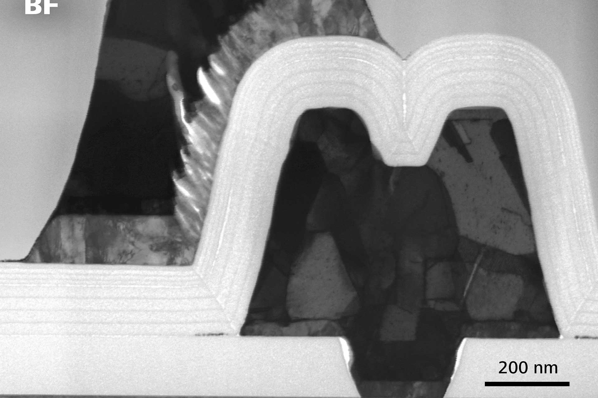

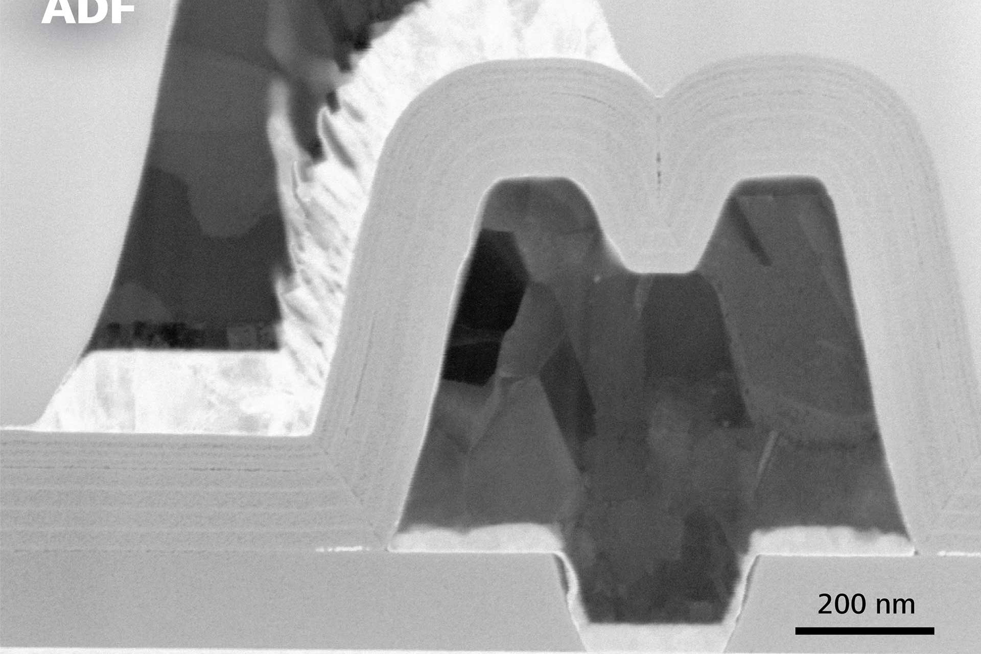

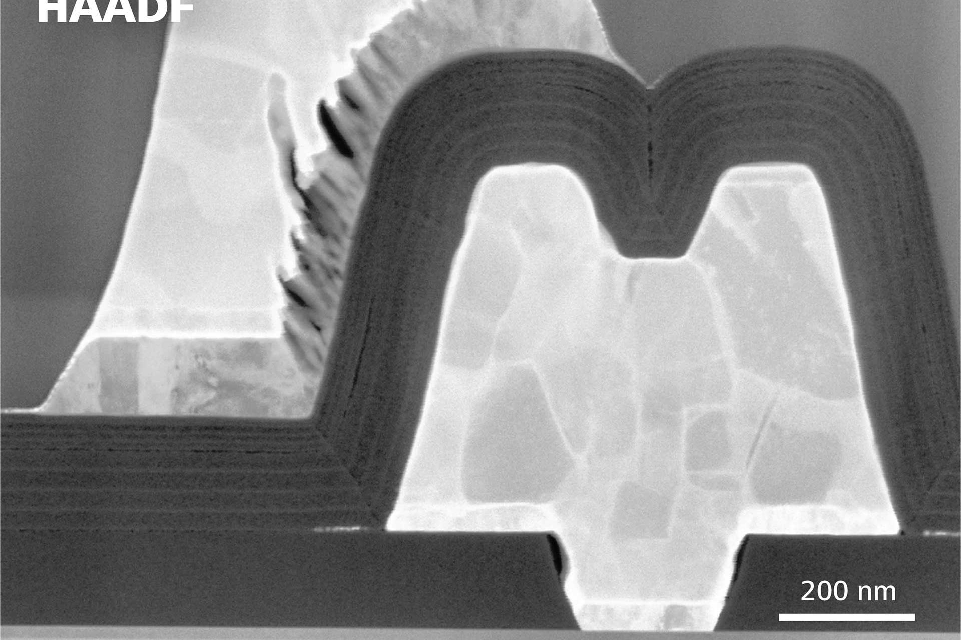

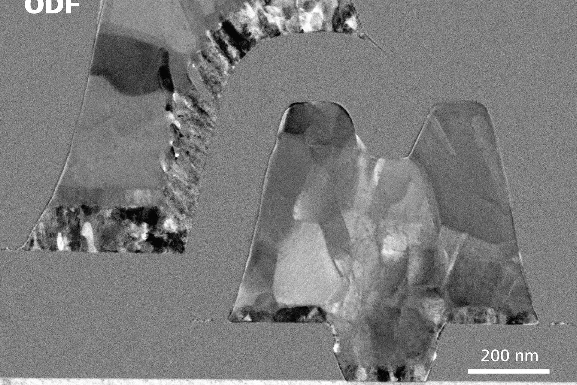


Cross Section and EDX of IGBT Device


Cross Section and EDX of IGBT Device
Examination of the edge of a gate in an Insulated Gate Bipolar Transistor (IGBT) device. Cross section and EDX elemental analysis performed entirely on a ZEISS Crossbeam 550 FIB-SEM. Brightfield 30 kV STEM-in-SEM image of lamella combined with EDX elemental mapping in Crossbeam revealed crystalline Si precipitates.


Dopant Profile Image of SiC MOSFET


Dopant Profile Image of SiC MOSFET
Cleaved SiC MOSFET device imaged at 1.5 kV in a ZEISS Crossbeam FIB-SEM. The image strongly highlights different implant doping regions due to the difference in work functions. The N+ diffusion is shown as a dark band underneath and extending to either side of the gate. The P-type body region is highlighted as a bright zone. This technique gives feedback on junction health and placement.
Nanoscale 3D X-ray Imaging of Smartphone Mainboard


3D Analysis of Smartphone Gyroscope / Accelerometer
3D Analysis of Smartphone Gyroscope / Accelerometer
3D X-ray reconstruction of silicon microcomb structures imaged at 1 µm/voxel resolution.
Acquired by ZEISS Xradia Versa X-ray microscope


High-resolution Image Fine Comb Fin
High-resolution Image Fine Comb Fin
Virtual plan view of same analysis showing fine comb fins imaged at 0.3 µm/voxel resolution.
Acquired by ZEISS Xradia Versa X-ray microscope


Virtual Slice of Fine Comb Fins
Virtual Slice of Fine Comb Fins
Virtual cross section of same sample showing a detailed view 2.1 µm fine comb fins imaged at 0.3 µm/voxel resolution.
Acquired by ZEISS Xradia Versa X-ray microscope
Non-destructive Analysis from System to Package to Interconnect


Smartphone


Smartphone
3D X-ray image of an entire smartphone image at 50 µm/voxel resolution.
Acquired by ZEISS Xradia Context microCT


Power Management IC Package


Power Management IC Package
Virtual plan view of power management integrated circuit (PMIC) package imaged at 11 µm/voxel resolution.
Acquired by ZEISS Xradia Context microCT


PMIC Interconnects


PMIC Interconnects Cross Section
Virtual cross section of PMIC solder bumps and vias imaged at 2.1 µm/voxel.
Acquired using the unique Resolution at a Distance capability of ZEISS Xradia Versa X-ray microscope


Analog Chip Imaged with EBAC
A digital counting chip examined with nanoprobing in a GeminiSEM at 20 kV. The Electron Beam Absorbed Current (EBAC) image contains information about the interconnectivity of sub-surface wiring and the buried p/n junctions.