Webinar
How EBL Enables High Quality Nanopatterning and Nanolithography
10 July 2025
· 70 min watch


Author
Ph.D. Kirill A. Atlasov
Product & Application Sales Specialist
Carl Zeiss Microscopy GmbH, Oberkochen, Germany
Carl Zeiss Microscopy GmbH, Oberkochen, Germany


Author
Dr. Frank Nouvertné
Senior Product Market Manager Electron Beam Lithography
Raith GmbH, Dortmund, Germany
Raith GmbH, Dortmund, Germany
Abstract
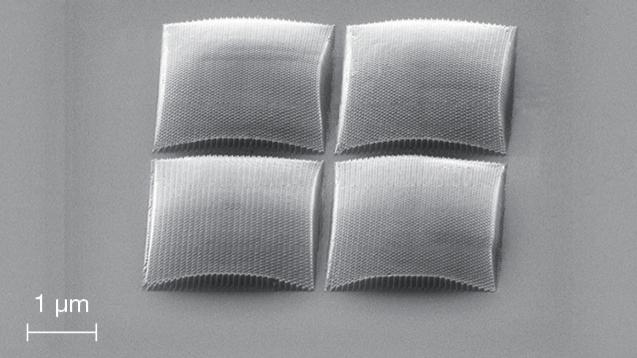
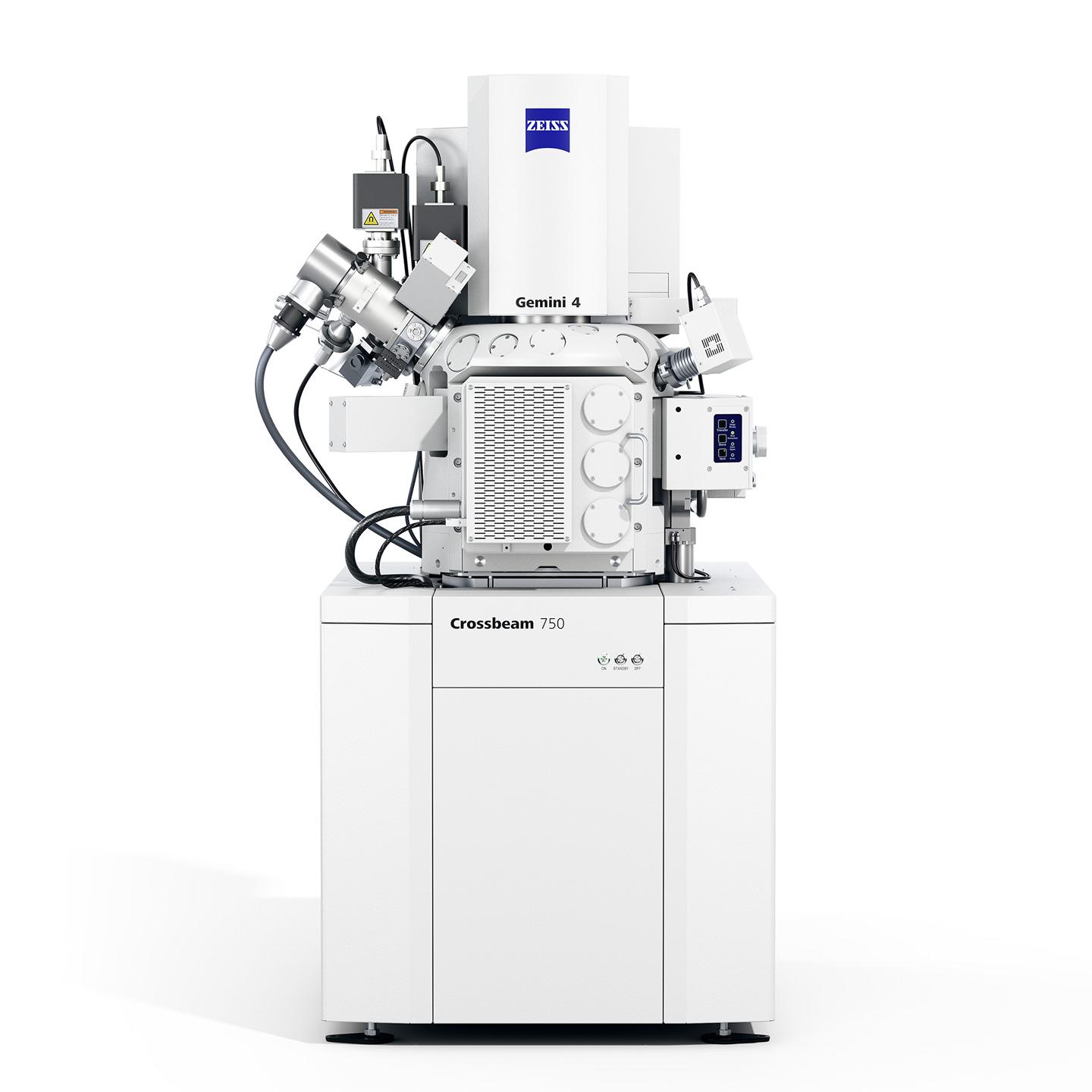
Today, research challenges in nanolithography and nanofabrication require cutting-edge solutions that leverage the latest advances in equipment for nanofabrication, nanostructuring, nanoobject imaging, and analysis. ZEISS field emission SEMs or FIB-SEMs with Gemini electron optics such as Crossbeam or GeminiSEM combined with RAITH ELPHY nanofabrication upgrade kits represent efficient and flexible solutions for the most diverse and novel research applications.
Join us for this webinar to learn more about ZEISS/RAITH EBL solution allowing the design of new materials and devices with new properties with high precision.
Key Learnings:
- How electron beam lithography (EBL) is used to design devices, systems and functional materials at the nano scale.
- How you can achieve proven reliability in nanolithography.
- How lithography attachments add value to the ZEISS FE-SEM and FIB-SEMs and extend the applications to nanolithography and nanofabrication without compromising their original functionality of imaging, analysis, or micromanipulation.
- The best use cases with application examples and recommendations for hardware.