How automated SEM workflows cut aerospace alloy testing from years to days
What if you could condense years of materials testing into just 13 days? At the National Institute for Materials Science (NIMS) in Japan, researchers have done exactly that. By transforming a process that traditionally takes over seven years into an automated workflow, they are reshaping the development of aerospace materials.
At NIMS’s Research Center for Structural Materials (RCSM), a team led by Toshio Osada in the High-Reliability Heat-Resistant Materials Group developed an automated high-throughput evaluation system. Postdoctoral researcher Dr. Thomas Hoefler and colleagues created a method that dramatically accelerates the generation of process-structure-property datasets, critical for designing high-performance materials in aerospace, energy, and structural engineering.
The method builds on foundational ideas developed by Dr. Takahito Ohmura, Head of the RCSM, and Dr. Toshio Osada, who envisioned multi-indentation and automated SEM workflows to accelerate structural materials research.
High-magnification SEM images of the approximately 1 µm indents are a key part of our method. There’s very little room for error in scan framing.
High-throughput microscopy: From basic metrics to complete characterization
Automation fundamentally changed how the team approaches alloy characterization. Previously, analyses were limited to basic metrics like phase area fractions and mean precipitate diameters. Now, they evaluate precipitate shapes, inter-precipitate distances, and size distributions across temperature ranges.
The results speak for themselves: 2,400 data points correlating processing conditions, microstructure, and yield strength – gathered in just 13 days.
Traditional tensile testing would take over 200 times longer.
Being able to set the sample for automatic SEM imaging on a Friday and review the data on Monday was a pivotal moment. It showed us the scale and depth of analysis we could achieve.
Automated SEM and nanoindentation
The complete workflow
Watch how the automated SEM and nanoindentation workflow operates in practice
Capturing thousands of data points in just days
Third-party Content Blocked
The video player is blocked due to your cookie preferences. To change the settings and play the video, please click the button below and consent to use of "Functional" tracking technologies.
Automated quad-channel AsB for indent pileup topography
Automated workflow
Four-channel Angular selective Backscatter (AsB) quad-mode image of an indent at 10 kV. The channels allow reconstructing 3D surface topography, which contains information on mechanical properties.
Superalloy microstructure before (top) and after (bottom) automatic image analysis. In-Lens, 1 kV.
Automated SEM analysis and nanoindentation of just one gradient-treated sample results in a complete Process-Structure-Properties dataset, containing information essential for structural materials.
High‑throughput SEM and nanoindentation reveal structure and properties at scale
From 3D indent topography to γ′‑microstructure maps and complete workflow integration
This automated workflow combines nanoindentation, SEM imaging, and image‑based analysis to produce a unified process–structure–property dataset from a single gradient‑treated specimen.
Mechanical response is captured through 3D topography of each indent, while γ′ precipitate size, shape, and fraction are derived from automated microstructure segmentation.
All results are linked through the same fully automated acquisition pipeline, enabling consistent high‑volume data generation for materials design.
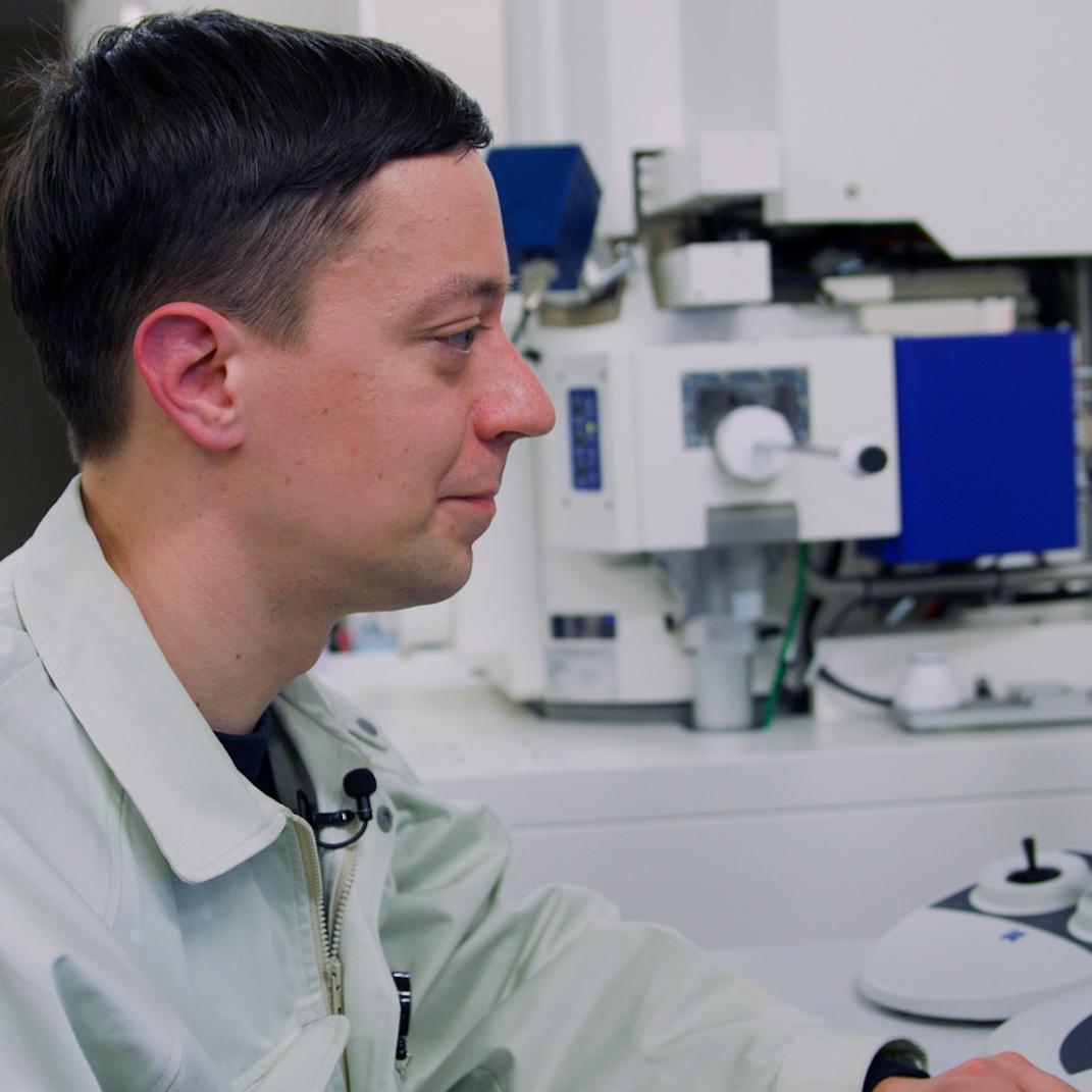
ZEISS GeminiSEM 300 in operation, providing high‑resolution imaging and automated acquisition for advanced materials characterization.
ZEISS GeminiSEM 300: Advanced automation for materials science
At the heart of this workflow is ZEISS GeminiSEM 300. Its SmartSEM Remote API provides full access to SEM parameters and live scan images, enabling automated imaging routines and real-time optimization based on local microstructure.
The Inlens secondary electron detector delivers high-contrast and high-resolution images – even under challenging conditions. In the team’s superalloy samples, γ and γ′ phases are nearly identical in composition and structure. Typically, metallographic etching is required to distinguish them – but not here.
This capability allowed the team to replace much of their transmission electron microscopy (TEM) workflow with SEM, enabling automated imaging and precipitate size analysis – even for features just tens of nanometers in diameter.
The AsB detector adds another layer: it produces 3D topographic images in a single scan. This proved essential for pile-up analysis in nanoindentation inverse modeling – traditionally done using atomic force microscopy.
The complete freedom of access via the API offered by ZEISS is vital to our research.
Collaborative development: From vision to publication
In 2021, Dr. Takahito Ohmura and Dr. Toshio Osada secured funding from Japan's ATLA* to develop multi-indentation combined with 3D SEM imaging. Dr. Ohmura procured ZEISS GeminiSEM 300 and automation infrastructure.
NIMS collaborated with System in Frontier Inc. on the GUI development and with graduate student Eri Nakagawa on workflow testing. Within ZEISS, Dr. Etsuo Maeda contributed to the development of the machine‑learning–based image‑recognition algorithms. This successful work was supported by the National Security Technology Research Promotion Fund of the Acquisition, Technology & Logistics Agency.
Dr. Thomas Hoefler joined as postdoctoral researcher to lead version 2 development – refining workflows and integrating advanced image analysis. Electron microscopy facility manager Dr. Toru Hara provided essential infrastructure support, maintaining NIMS's long-standing ZEISS collaboration. Former member Takuma Kohata also contributed during the early development phases.
*Acquisition, Technology & Logistics Agency in Japan, an organization under the Japanese Ministry of Defense
Process-structure-property datasets: Accelerating aerospace materials development
For NIMS, the impact is clear: a process that once took over seven years can now be completed in under two weeks – freeing up resources, accelerating discovery, and enabling more confident design decisions.
The team’s method supports the development of improved predictive models for phase composition and mechanical properties – especially valuable in aerospace, where complex alloys and extreme temperatures challenge existing databases.
In a study on the nickel-cobalt base superalloy TMP-5002, the system captured measurements at 220 different aging temperatures (647°C to 1,208°C), analyzing nearly one million individual γ′ precipitates. This enabled detailed coarsening kinetics analysis and application of advanced theoretical models with high confidence.
Seeing the subtle changes in the precipitate size distribution shapes with processing conditions was memorable, made possible by the large number of precipitates imaged.
The team is now exploring automated Energy Dispersive X-ray Spectroscopy (EDS) and Electron Backscatter Diffraction (EBSD) to include composition and crystallographic data. They’re also investigating in-situ SEM nanoindentation for high-temperature mechanical testing – critical for aerospace materials that must perform under extreme conditions.
By combining SEM imaging, nanoindentation, and open-source software, the team has built a scalable, high-throughput workflow that delivers consistent, highly correlated data. All analyses are performed on the same sample in a single session, eliminating environmental and operator-related variation – an advantage over traditional multi-sample studies.
The method is applicable to any engineering material accessible to SEM and nanoindentation, making it a powerful tool across the full spectrum of structural materials development.
We hope that wide adoption of high-throughput experimental methods will lead to improved databases for predicting equilibrium phase composition and mechanical properties. Even today, state-of-the-art commercial databases often fail to make reliable predictions for the complex alloys in actual use.
Explore the full studies
Dive into the complete methodology and results in this publication:
Automated system for high-throughput process-structure-property dataset generation of structural materials: A γ/γ′ superalloy case study, published in Materials & Design (2025), Volume 249, Article 114279
This work builds on earlier research by Dr. Ohmura and Dr. Osada, including the foundational study:
High-throughput evaluation of stress–strain relationships in Ni–Co–Cr ternary systems via indentation testing of diffusion couples, published in Journal of Alloys and Compounds (2022), Volume 918, Article 165829
About the Research Center for Structural Materials
The Research Center for Structural Materials (RCSM) at NIMS Japan conducts research on structural materials with a focus on both material development and evaluation. The center’s current strategic plan emphasizes materials for extreme environments and advanced evaluation technologies for structural performance.Its team develops materials for conditions such as cryogenic temperatures, high heat, and seismic stress, and advances methods like multi-scale measurement and computational modeling to better understand material behavior.
RCSM also supports collaboration across industry, academia, and government, and contributes to standardization and accident analysis in structural materials.
Automated high-throughput testing using gradient samples reduces characterization time by up to 200x. Instead of testing thousands of specimens, analyze a single sample with multiple processing conditions. NIMS generated 2,400 data points across 220 temperatures in 13 days – traditionally requiring over seven years – while eliminating sample-to-sample variation.
Yes. Combining automated SEM imaging with nanoindentation inverse analysis calculates stress-strain curves from microscale indents
(~1 µm), eliminating machined tensile specimens. NIMS generated 2,400 stress-strain curves in 13 days – 200x faster than traditional tensile testing – while correlating mechanical properties directly to microstructure at identical sample locations.
Open API access to microscope parameters and live scan images is essential. ZEISS GeminiSEM 360's SmartSEM Remote API enables full automation of imaging routines with real-time optimization. The InLens detector distinguishes phases without etching, while the four-channel AsB detector generates 3D topography in a single scan – critical for high-throughput analysis.