Two employees from the SMT Semiconductor Fab Solutions segment chat in the ZEISS SMT clean room
Semiconductor Fab Solutions (SFS)  

Accelerated processes Wafer fab solutions for next generation semiconductor elements

New Designs for chips and chiplets, increasing complexity, new materials, and ever smaller semiconductor structures: ZEISS Semiconductor Manufacturing Technology (SMT) provides inspection, metrology and defect analysis solutions that enable the advanced manufacturing of logic and memory chips and thus meet ever-increasing demands.

  • 3D Metrology and Inspection Workstation
  • ZEISS MultiSEM
Electron beam of the MultiSEM technology from ZEISS SMT

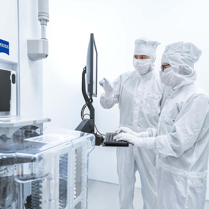
Valuable information Inspection, metrology and defect analysis for new methods

With its wide range of technologies, ZEISS SMT offers innovative wafer fab solutions for obtaining relevant information for the production of logic and memory chips. This is how we equip the semiconductor industry to meet its challenges for the next generation of elements.

Faster, more precise, and more flexible Our solutions designed for wafer production

  • 1,5 TB

    Constant data rate per hour with ZEISS MultiSEM

  • 0,9 nm

    SEM resolution at the coincidence point at 15 kiloelectron volts (keV) with the 3D Metrology and Inspection Workstation

ZEISS SMT wafer fab solutions at a glance

A 3-D Tomo Metrology Workstation form ZEISS SMT

ZEISS 3D Metrology and Inspection Workstation

The ZEISS 3D Metrology and Inspection Workstation is a FIB-SEM combination for 3D high-throughput analysis with a resolution of up to 0.9 nanometers. This allows you to analyze the volume of microchips – sampling, analyzing and validating with nanometer accuracy.

Two employees work on the MultiSEM

ZEISS MultiSEM

With 91 parallel electron beams, the unique, highly efficient ZEISS MultiSEM multi-beam scanning electron microscope makes complex 2D structures visible at an incomparably high speed. The intuitive ZEISS ZEN Imaging software enables reverse engineering, process control and troubleshooting in the finest semiconductor structures.

Anything is imaginable – a lot is possible Contact us today

ZEISS SMT empowers manufacturers worldwide with lithography optics and solutions for high-volume wafer production for semiconductor manufacturing. With increasing complexity, new materials and the miniaturization of semiconductor structures, the demands on inspection, metrology and defect analysis systems ar ealso rising.

For further information please contact our experts.