

Products from ZEISS Semiconductor Manufacturing Technology
Making tomorrow’s technologies possible today
What do smartphones, AI, and quantum computing have in common? They rely on semiconductor technology with circuits in the nanometer range. With the product portfolio for semiconductor manufacturing, the ZEISS segment Semiconductor Manufacturing Technology (SMT) covers various phases of chip development and production. We enable the semiconductor industry worldwide for the next technological leap. For this, we constantly push the boundaries of what is technologically possible – and move them forward.Discover our portfolio
ZEISS Semiconductor Manufacturing Technology

Lithography optics
With lithography optics, laser optics, mirror blocks, and other optical systems, we enable customers worldwide to expose wafers with a resolution in the nanometer range. This creates the foundation for ever smaller, more efficient, and more powerful microchips. ZEISS SMT optics and mirrors are also used in synchrotrons for fundamental physical research.


Photomask solutions
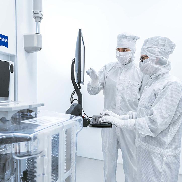
Error-free exposure of wafers in semiconductor production saves time and money. With our photomask solutions, defects on the photomask can be detected, analyzed, and repaired, as well as specific mask properties measured and optimized. This enables the production of defect-free photomasks for microchip manufacturing.


Wafer fab solutions
Ensuring wafer shape and detecting critical defects require precise metrology and process control throughout the fab. Our wafer fab solutions enable sample preparation, global wafer shape control, and nanometer-accurate structure and defect review. Highly efficient 2D and 3D imaging solutions enable manufacturers to stabilize processes and safeguard yield – from front-end processing through advanced packaging.


Interesting facts from the semiconductor industry
ZEISS Semiconductor Manufacturing TechnologyFrequently Asked Questions
-
Our everyday life is becoming increasingly digital, smarter, more connected – and computing power is continually increasing. This is only possible with microchips. The product portfolio of ZEISS SMT covers various key processes in the production of microchips, including semiconductor manufacturing solutions – such as lithography optics, photomask systems, as well as solutions for the production of leading-edge microchips and chiplets. This way, we enable chip manufacturers worldwide and lay the foundation for ever smaller, more powerful, and energy-efficient microchips globally. The electronic applications equipped with these microchips enable global progress in various disciplines. Microchips are built into electronic products, found in almost every household appliance, such as dishwashers or coffee machines. Devices like smartphones, computers, or tablets cannot function without them. And technological innovations like automation, AI, or autonomous driving would be unimaginable without them.Thus, ZEISS SMT shapes technological progress and makes things possible that we do not yet know today.
More information about ZEISS SMT
-
ZEISS Semiconductor Manufacturing Technology (SMT) consists of three strategic business units (SBUs). Together, they form the product portfolio of ZEISS SMT and deliver key technologies for microchip manufacturing:
SMO – Semiconductor Manufacturing Optics
SMS – Semiconductor Mask Solutions (photomask solutions for semiconductor manufacturing)
SFS – Semiconductor Fab Solutions (solutions for high-volume wafer production) -
Within ZEISS Semiconductor Manufacturing Optics (SMO), we develop and manufacture highly precise optical systems and technologies for the semiconductor industry. The portfolio includes lithography optics (for DUV, EUV, and High-NA-EUV lithography) and illumination systems, laser optics, optical modules for wafer and mask inspection, as well as synchrotron optics and X-ray gratings for research applications. These solutions enable chip manufacturers to expose the finest structures and are crucial for the production of powerful microchips.
-
Within ZEISS Semiconductor Mask Solutions (SMS) we offer high-end solutions for the production of photomasks. The portfolio includes mask metrology, tuning, qualification, and repair solutions that cover a wide range of mask types and lithography techniques in the DUV and EUV spectral range – for maximum efficiency in semiconductor manufacturing and maximum yield of defect-free, functional microchips per wafer.
-
Semiconductor Fab Solutions (SFS) offers highly precise systems for inspection, metrology, defect analysis, and wafer shape control in semiconductor manufacturing.
The portfolio includes ZEISS INTUITIVE 3D and EXPLORE 3D, FIB-SEM combinations for fast nanometer-accurate sampling and 3D analyses; ZEISS MultiSEM, a unique multi-beam scanning electron microscope with 91 parallel electron beams for fast high-resolution 2D analyses; ZEISS NLX, an in-line 3D X-ray laminography system for non-destructive inspection and metrology of advanced packaging structures; and ZEISS DUNE, a wafer shape control solution combining integrated metrology with active warpage correction.
These solutions provide critical information for analysis, process optimization, and problem resolution for faster and more efficient manufacturing of finest microchip structures.
-
Germany
- Oberkochen (Baden-Württemberg): Headquarters and central R&D, and production site for lithography optics (ZEISS SMO)
- Jena (Thuringia): At the ZEISS founding site, optical mask systems are developed, and mask repair, qualification, and metrology systems of ZEISS SMS are manufactured.
- Wetzlar (Hesse): Production site for lithography optics
- Rossdorf (Hesse): R&D site for ZEISS SMS, focusing on mask repair systems
- Aachen (North Rhine-Westphalia): R&D site
- Coswig (Saxony): Site for development and production
International
- Zurich (Switzerland): Site for development and production
- Dublin (USA): R&D site for ZEISS SFS
- Bar Lev (Israel): R&D site for ZEISS SMS, focusing on mask tuning systems
Additionally, we have our sales and service companies (SSCs) in the US, China, Taiwan (region), South Korea, and Japan:
- USA: Dublin (SSC), Phoenix, Boise, Hillsboro (ZEISS SMS service locations)
- China: Shanghai (SSC), Jinan (ZEISS SMS service location)
- Taiwan (Region): Hsinchu (SSC), Tainan, Taichung (ZEISS SMS service locations)
- South Korea: Seoul (SSC), DongTan, Pyeongtaek (ZEISS SMS service locations)
- Japan: Tokyo (SSC)
Strong together
Our partner and supplier network of ZEISS Semiconductor Manufacturing Technology

Markets and Partners
ZEISS SMT equips the semiconductor industry worldwide with its technology solutions – and is a pace-setter for digitalization. This is achieved with a strong network of more than 1,200 partners and suppliers.


Supplier network
With the supply chain strategy, the supplier management of ZEISS Semiconductor Manufacturing Technologies (SMT) coordinates, controls, and shapes the value creation of our suppliers. ZEISS SMT aligns itself with the requirements of our customers in the OEM and end-user markets.