ZEISS AIMS EUV 3.0: New Generation Triples Mask Throughput
- The new generation of the AIMS® EUV 3.0 mask qualification tool from ZEISS SMT has been successfully established on the market.
- Customers benefit from high uptime, full performance, and cost-optimized features.
- The future-proof platform supports the wafer scanner roadmap with Low-NA EUV and High-NA-EUV technology.
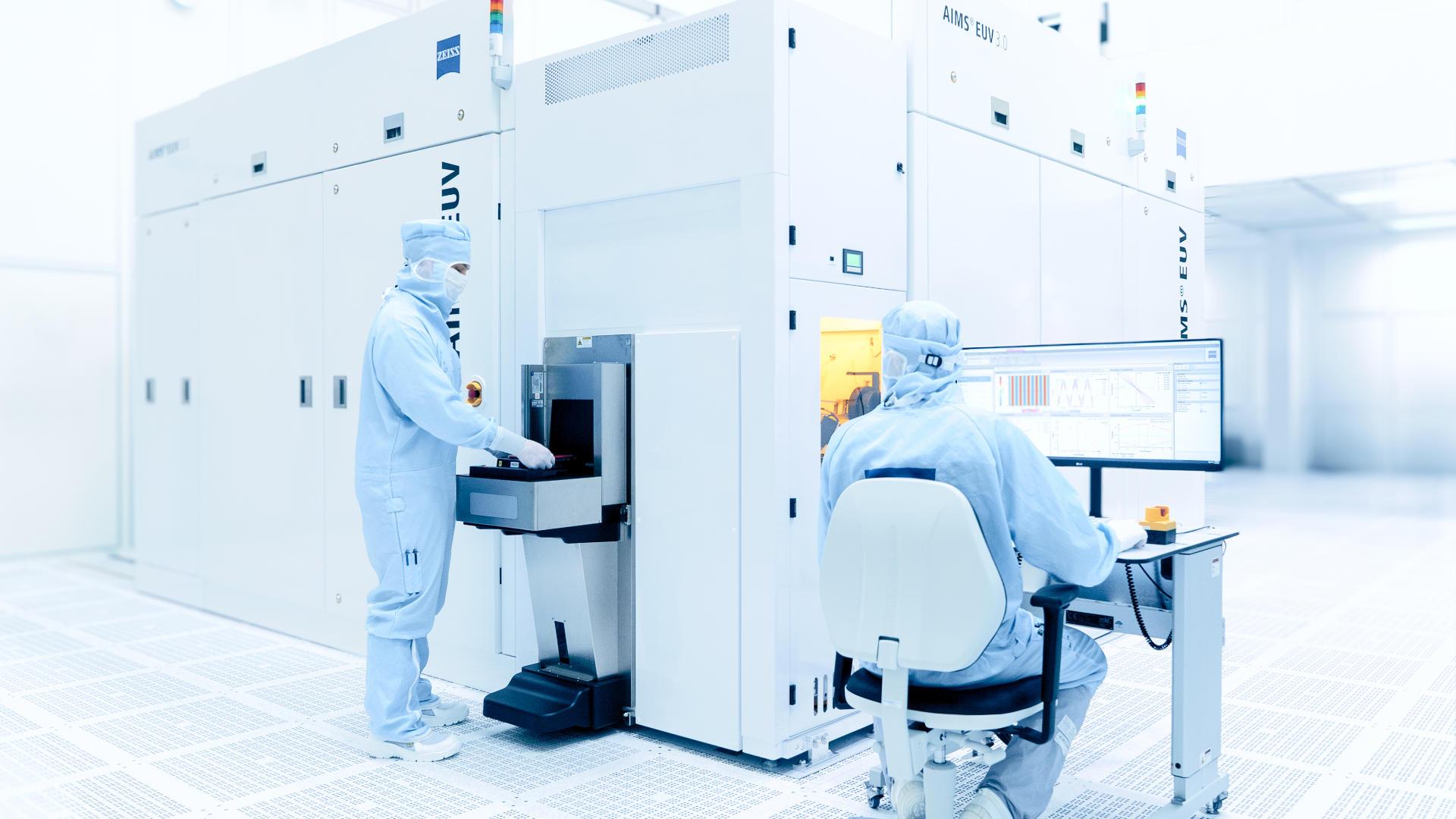
ZEISS AIMS systems (Aerial Image Measurement Systems) have been setting standards in mask qualification for over 30 years. Now, the Semiconductor Manufacturing Technology (SMT) segment of ZEISS has successfully introduced the new generation AIMS® EUV 3.0 to the market. The system supports both Low-NA EUV and the advanced High-NA-EUV technology, significantly increases productivity, and enables a threefold increase in mask throughput. Initial systems are already in use at chip manufacturers and are meeting expectations for performance and availability.

The latest generation of the ZEISS AIMS® EUV 3.0 system significantly triples mask throughput. The cutting-edge platform is designed to support both Low-NA and High-NA EUV lithography, and has already proven its success in the market.
ZEISS SMT has consolidated its photomask expertise within the strategic business unit Semiconductor Mask Solutions (SMS). “The photomask is the heart of lithography and therefore a key driver of performance in modern microchips,” says Dr. Clemens Neuenhahn, Head of ZEISS SMS. Defect-free photomasks are essential for cost-effective and sustainable microchip production. Chip manufacturers review mask defects before they are used in wafer steppers and scanners, allowing potential impacts on printability to be identified early and corrected.
ZEISS AIMS EUV is a proven tool that evaluates the printing performance of EUV masks and replicates the imaging characteristics of scanners. With the new generation AIMS® EUV 3.0, ZEISS SMT is addressing the industry’s increasing demand for more productive systems and optimized cost structures.
“With AIMS® EUV 3.0, we’re offering a future-proof solution that delivers technological excellence and creates real added value for our customers in everyday production – through higher productivity, flexibility, and operational reliability,” says Neuenhahn.
High Availability and Full Performance in Ongoing Operation
ZEISS has delivered, installed, and successfully commissioned the first two systems of the new AIMS® EUV generation at two chip manufacturers. In operation, they meet technical expectations and impress with high availability, stable performance, and optimal efficiency.
“The positive customer feedback confirms that with AIMS® EUV 3.0, we are addressing the requirements that are crucial for the next generation of semiconductor manufacturing. It motivates us to continue this journey together with our customers and partners,” says Dr. Axel Zibold, Head of Sales & Customer Support at ZEISS SMT.
Future-Proof Platform for Low-NA and High-NA-EUV Lithography
AIMS® EUV 3.0 is based on the proven optical design of its predecessor and is fully compatible with High-NA-EUV technology. The platform supports imaging for both Low-NA technology (0.33NA isomorphic) and High-NA-EUV technology (0.55NA anamorphic). This enables chip manufacturers to respond more flexibly to varying requirements and secure strategic advantages along their roadmaps.
At the same time, they benefit from enhanced features: the new AIMS® generation triples mask throughput compared to the previous version, thereby increasing productivity. Another key feature is flexible illumination, which allows for customized light settings tailored to specific mask requirements. This makes it possible to replicate even complex EUV scanner settings.