Deutscher Zukunftspreis 2020: EUV developers from TRUMPF, ZEISS and Fraunhofer nominated
Ditzingen/Oberkochen/Jena, Germany | 9 September 2020 | ZEISS Semiconductor Manufacturing Technology
- EUV lithography enables most modern smartphones and automated driving
- World-leading manufacturing technology strengthens German-European position in global semiconductor business
The Office of the Federal President today announced the nominees for the Deutscher Zukunftspreis 2020 (German Future Prize 2020) in the Ehrensaal of the Deutsches Museum in Munich. The circle of the best - the three projects for the final round of the German President's Award for Technology and Innovation - includes a team of experts from TRUMPF, ZEISS and Fraunhofer IOF: With their project "EUV Lithography - New Light for the Digital Age", Dr. Peter Kürz, ZEISS Semiconductor Manufacturing Technology (SMT) segment, Dr. Michael Kösters, TRUMPF Lasersystems for Semiconductor Manufacturing, and Dr. Sergiy Yulin, Fraunhofer Institute for Applied Optics and Precision Engineering IOF in Jena, have been nominated.
More powerful, energy-efficient and cost-effective chips
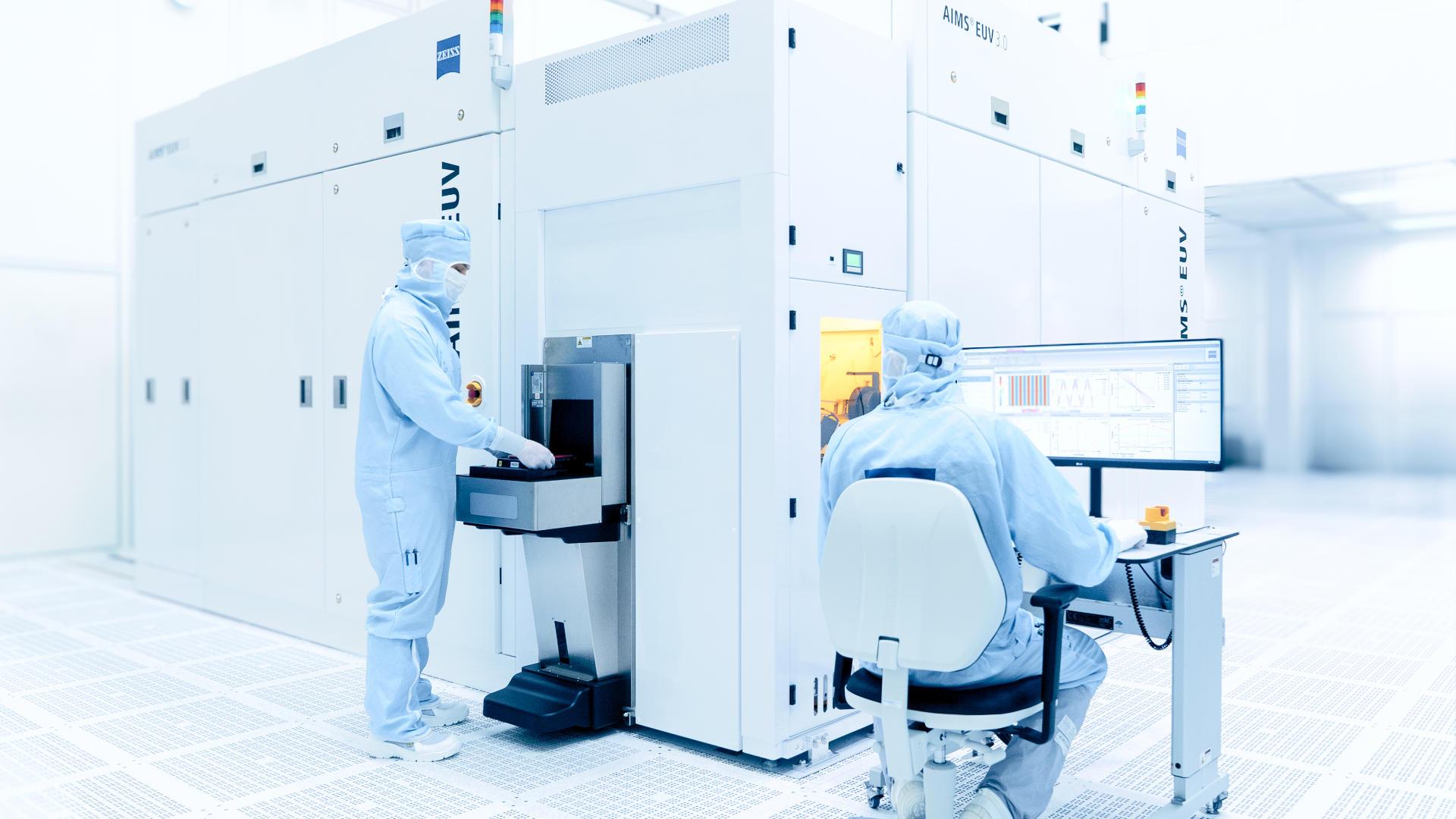
The world's only manufacturer of EUV lithography machines is the Dutch company ASML, which as integrator designed the architecture of the overall system and in particular the EUV source. Key components of these machines are the high-power laser from TRUMPF for the EUV light source and the optical system from ZEISS. EUV stands for "extreme ultraviolet", i.e. light with an extremely short wavelength. With this technology, far more powerful, energy-efficient and cost-effective microchips than ever before can be produced. After all, successful digitization cannot be achieved without a further sharp increase in computing power. Today, a smartphone already has millions of times the computing power of the devices that accompanied the first moon landing in 1969. This is made possible by a microchip barely the size of a fingertip, which contains more than ten billion transistors. The production process for the latest chip generations is based on the use of EUV light, which overcomes previous limits of what is technically possible. From the light source to the optical system in a vacuum to the surface coating of the mirrors used in this process, practically the entire exposure technology had to be developed from scratch.
Future technology in industrial series application
The three nominees have made a significant contribution to the development and industrial maturity of the EUV technology. The result is a future technology secured by more than 2,000 patents, which is the basis for future technical progress and the digitalization of our everyday life.


TRUMPF Vice Chairman of the Group Management Board and Chief Technology Officer Peter Leibinger: "We are very pleased with the nomination for the Deutscher Zukunftspreis. It confirms once again the worldwide potential of EUV technology. Thanks to our partnership with ZEISS, Fraunhofer and the Dutch technology group ASML, we were able to prevail in Germany and Europe against competitors from Japan and the USA for this future technology. The fact that the world's best machines for manufacturing microchips come from Europe is an extraordinary story that we have written together. The key to the success of this unique cooperation is mutual trust and staying power".
With the world's strongest pulsed industrial laser, TRUMPF supplies a key component for the exposure of the most modern microchips used in every modern smartphone. There is no economical alternative to this laser for generating the light required for EUV lithography. Leibinger: "Only TRUMPF can build the lasers needed for EUV lithography. Without these lasers, future technologies such as artificial intelligence or automated driving could not be implemented because they require a lot of computing power. The nomination for the Deutscher Zukunftspreis on the occasion of the laser's 60th birthday once again underlines the enormous importance of this tool for Germany as an industrial location".
"Together with our partners, we are very pleased about the nomination, which recognizes an enormously complex development effort and its translation into a technology that dominates the global market," says Dr. Markus Weber, member of the ZEISS Group Management Board and head of the Semiconductor Manufacturing Technology segment. "ZEISS stands for outstanding optical performance and precision. This has always been a key factor in chip production. EUV technology with its vacuum-operated mirror optics is a leap-frog innovation that required both creativity and perseverance to get from the idea to today's series production. The quality and shape of the illumination system and the resolution of the projection optics determine how small structures on microchips can be. EUV continues to enable major advances in digitization in business and society. We are proud to contribute to this together with our strategic partner ASML, TRUMPF and Fraunhofer".
Essential innovations are embedded in the mirrors. Since even the smallest irregularities lead to imaging errors, the world's "most precise" mirror was developed for EUV lithography. Fraunhofer was an important research partner in the sophisticated coating technology for the mirrors.
"Fraunhofer is one of the pioneers in semiconductor technology. At our institutes and facilities, we have been researching in the field of EUV lithography for three decades. Our researchers played a major role in the development of the first EUV mirrors and beam sources, thus laying the foundation for the breakthrough of this technology," explains Prof. Reimund Neugebauer, President of the Fraunhofer-Gesellschaft. "Thanks to the intensive and long-standing cooperation between science and industry, we have now succeeded in making the leap to broad application in this innovative field worldwide. EUV lithography is an outstanding example of the technological and economic added value that can be achieved through cooperation, a spirit of research and sustained commitment".