Thin Films
Sub-Nanometer Imaging of Sensitive Materials Below 1 kV Without an Immersion Lens, Beam Damage, or Charging EffectsLike most nanomaterials with dimensions approaching the quantum realm, thin films demonstrate properties not seen in their bulk counterparts. Atomic scale processing techniques like ALD or ALE can now deposit (or remove) materials one atomic layer at a time, allowing extreme control over feature sizes during device fabrication. And understanding the surfaces and chemistry of these films is critical to optimizing their performance.
Advancing Nanomaterials Research - One Atomic Layer at a Time
But one of the major challenges in thin film research is imaging surfaces at high resolution without introducing specimen damage. Gaining accurate, high resolution chemical data from these same samples using EDS is also problematic, due to extremely low X-Ray counts.
Higher Resolution at Lower kV is the Solution
Solving these problems has pushed the development of SEM tools that allow higher resolution imaging at lower and lower kV. In fact, high performance SEM imaging below 1 kV is now considered the gold standard when analyzing thin film materials. And if you combine this with high resolution EDS mapping using advanced detector systems (that maximize the solid and take-off angles), you can also glean highly accurate chemical data from these surfaces too. In turn, this gives you confidence that your EDS spectrum or map is an accurate representation of your sample.
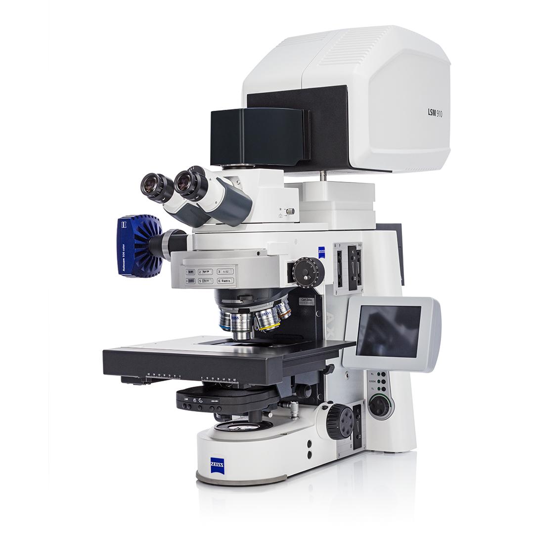
ZEISS SEMs and LMs Help You Make Progress
ZEISS continues to develop low-kV, high resolution imaging technology so you can push your research forward. ZEISS GeminiSEMs, combined with EDS detectors specifically designed for the Gemini optical SEM columns, help you analyze the surface of beam-sensitive thin films with never-before-seen resolution. Additionally, fast and non-destructive 3D-topographic measurements can be performed optically - with confocal laser scanning techniques.


Automatic detection of fluorescently labelled cell nuclei in biological samples with ZEISS ZEN


Automatic detection of fluorescently labelled cell nuclei in biological samples with ZEISS ZEN
Automatic detection of fluorescently labelled cell nuclei in biological samples with ZEISS ZEN
Robust and Reliable Data
Success in Drug Discovery
The ZEISS solutions for high-content imaging facilitate generation of consistent data through many facets.
- First, the ZEISS Celldiscoverer 7 market leading imaging technology generates high quality data with the gentlest possible imaging, protecting your samples from light-induced perturbations.
- Additionally, ZEISS provides high-quality training and support resources to enable even novice users to utilize the technology to its full potential, setting them up for success right from the start.
- Beyond that, both ZEN image acquisition parameters and ZEISS arivis Pro image analysis pipelines can be incorporated in fully automated workflows, rendering data output fully consistent and reproducible across users and throughout the timescale of your study.
- Finally, the scalable ZEISS arivis Hub analysis and data management platform includes transparent user management and audit trail functionality to ensure complete traceability of your results, even when dealing with excessively large and complex datasets.
Applications


Trace Elements in Thin Films


Trace Elements in Thin Films
Perovskite solar cell on a glass substrate after a top-down SIMS measurement. ROI was scanned by the gallium beam 500 times. Secondary ions were analyzed spectroscopically according to their mass/charge ratio. A significant Na signal is observed across all layers. Intermixing and diffusion of trace elements can be studied by SIMS and is known to influence the performance of thin-film photovoltaic cells. (left SEM image, scale bar 2μm, right Na SIMS map). ZEISS Crossbeam 350 FIB-SEM with a Time of Flight (ToF) SIMS detector. Sample courtesy of Arafat Mahmud, RSEEME, Australian National University.
ZnO Nanoparticles on a Carbon Film
STEM tilt series, brightfield STEM images are shown as one example of four signals collected in total simultaneously with the aSTEM detector using the special sample holder for STEM tomography. ZEISS GeminiSEM.