New multifunctional factory for ZEISS in Wetzlar
- Megatrends are generating high demand for semiconductor manufacturing equipment and necessitating an increase in production capacity.
- A new multifunctional factory in the Dillfeld district of Wetzlar will extend over more than 12,000 square meters and offer flexible work areas with a low-vibration design for optics, coating and assembly.
- 150 new production and development jobs will be created.
The groundbreaking ceremony on March 29, 2023, marks the start of construction work for the expansion of the ZEISS Semiconductor Manufacturing Technology (SMT) segment’s Wetzlar site. In the future, an area of over 12,000 square meters will be devoted to the development and manufacture of lithography optics for global microchip production. This expansion is ZEISS’s response to the worldwide growth in demand for microchips in the semiconductor industry.


, Christoph Hensche (Chief Operating Officer and Digital Transformation Officer ZEISS SMT), Dr. Andreas Viertelhausen (Mayor of Wetzlar), Katrin Ariki (Site Manager ZEISS SMT in Wetzlar), Manfred Wagner (Chief Mayor of Wetzlar) and Rainer Dietrich (Economic Development Wetzlar) at the groundbreaking ceremony for ZEISS’s new multifunctional factory in Wetzlar. (Photo: ZEISS / Andreas Bender)")
, Christoph Hensche (Chief Operating Officer and Digital Transformation Officer ZEISS SMT), Dr. Andreas Viertelhausen (Mayor of Wetzlar), Katrin Ariki (Site Manager ZEISS SMT in Wetzlar), Manfred Wagner (Chief Mayor of Wetzlar) and Rainer Dietrich (Economic Development Wetzlar) at the groundbreaking ceremony for ZEISS’s new multifunctional factory in Wetzlar. (Photo: ZEISS / Andreas Bender)")
Megatrends generating strong demand for microchips
The megatrends associated with digitalization – Industry 4.0, autonomous driving and 5G – mean more and more microchips are required. “We are seeing an ever-growing market demand for semiconductor manufacturing equipment. Our lithography optics enable chip manufacturers worldwide to produce microchips with nanometer precision,” says Wetzlar’s Site Manager Katrin Ariki. Wetzlar has been one of ZEISS’s production sites for DUV lithography optics for over twenty years, but the existing production capacities are now reaching their limits.
New multifunctional factory will expand development and production capacity
The new building located in the Dillfeld industrial zone will complement the existing site in downtown Wetzlar, which is also being renovated. “We tested various new concepts for automating our production at the existing site and are now incorporating the findings into the new building,” explains Ariki. In the future, around 150 skilled staff will manufacture products such as ultramodern DUV illumination systems in a production area of more than 12,000 square meters. The building must therefore meet specific requirements. “Nanometer precision is a must for our products, so we are paying particular attention to ensuring a vibration-free building design for our sensitive measurement technology,” continues Ariki. The new factory is also being geared toward maximum flexibility. “We can easily adapt the work areas for optics, coating and assembly to new requirements,” she says. The office building will accommodate workshops, changing rooms, social facilities, a canteen as well as a cafeteria.
New jobs for the region
“During the current decade, we will need more microchips than ever before if we are to respond to the megatrends associated with digitalization. Besides building additional development and production facilities, we are therefore also recruiting further staff in both areas,” explains Ariki. Some 380 people are currently working for ZEISS SMT at its site in Wetzlar, compared to 170 in 2017, and the expansion is now creating space for an additional 150 staff. “When work is completed in 2025, our plan is that ZEISS SMT in Wetzlar will provide over 500 jobs,” reveals Ariki. In addition, the more than 100 employees of the ZEISS Consumer Products segment will continue to manufacture binoculars, spotting scopes and hunting optics at the current site.
Investment in the “city of optics”
“In Hesse, we very much appreciate having key research facilities such as the universities in Giessen, Marburg, Siegen and Frankfurt close by, so we feel very much at home in Wetzlar and are looking to continue growing here,” underlines Ariki. Wetzlar’s mayor Manfred Wagner is delighted about this commitment to the location. “ZEISS plays a major part in our branding as the ‘city of optics’. Its investment in expanding the site and creating new jobs sends out an important signal, especially in these challenging times. It shows that Wetzlar is an attractive location for companies and skilled professionals,” he says. “We would like to thank Wetzlar city council for its support with the planning and are looking forward to our future collaboration,” adds Ariki.
Part of ZEISS’s global growth strategy
The ZEISS Group is sticking to its long-term growth strategy and is expanding both in Germany and at many international locations. “Innovations and a growing workforce require space to develop,” insists ZEISS SMT’s Chief Operating Officer (COO) and Digital Transformation Officer (DTO) Christoph Hensche. ZEISS SMT is therefore also expanding its site in Rossdorf, in the southern part of Hesse. “By investing in people, infrastructure and technology at both locations, we are looking to help attract job seekers to the region,” emphasizes Hensche. The ZEISS Group is among the mainstays of Germany as an industrial location and is growing in all areas – from Jena and Dresden to Oberkochen, where ZEISS SMT is headquartered.
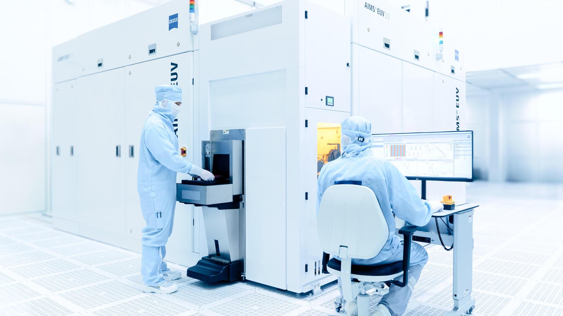
High-precision optics for global chip manufacturing
When manufacturing microchips, the structures are created on the wafers by exposing photomasks to short-wavelength light. The microchips are cut from these wafers and go on to be used in products such as computers. DUV (deep ultraviolet) technology and ultraviolet light are used in the vast majority of cases. ZEISS produces the necessary optics for wavelengths of 365, 248 and 193 nanometers. By way of comparison, the human eye can detect wavelengths ranging from around 380 to 780 nanometers. Over 80 percent of the world’s microchips are manufactured using these optics from ZEISS.