Press Release

Experience future technologies today: ZEISS at the W3+ Fair in Wetzlar

As a technology leader and employer in the Central Hesse region, ZEISS SMT takes part at this year’s W3+ Fair with ist own exhibition booth and presentation

12 March 2024 · 5 min read

  • At the W3+ Fair on March 13 and 14, 2024 in Wetzlar, Germany, ZEISS Semiconductor Manufacturing Technology (SMT) will talk about optical lithography and the next technological leap for the production of smaller, more powerful and more energy-efficient microchips
  • With ist high-tech products, ZEISS SMT is driving forward global digitalization and the use of AI
  • The company benefits from the optical expertise in Central Hesse as a business location
Wetzlar, Germany | 12 March 2024 | ZEISS Semiconductor Manufacturing Technology

This year, the ZEISS Semiconductor Manufacturing Technology (SMT) segment takes part in the W3+ Fair, which will take place from March 13 to 14, 2024, in the Buderus Arena in Wetzlar. ZEISS can be found at exhibition booth number A11 in the Buderus Arena and will also give a lecture on optical lithography and the next technological leap for the production of microchips on March 13 at 11 a.m.

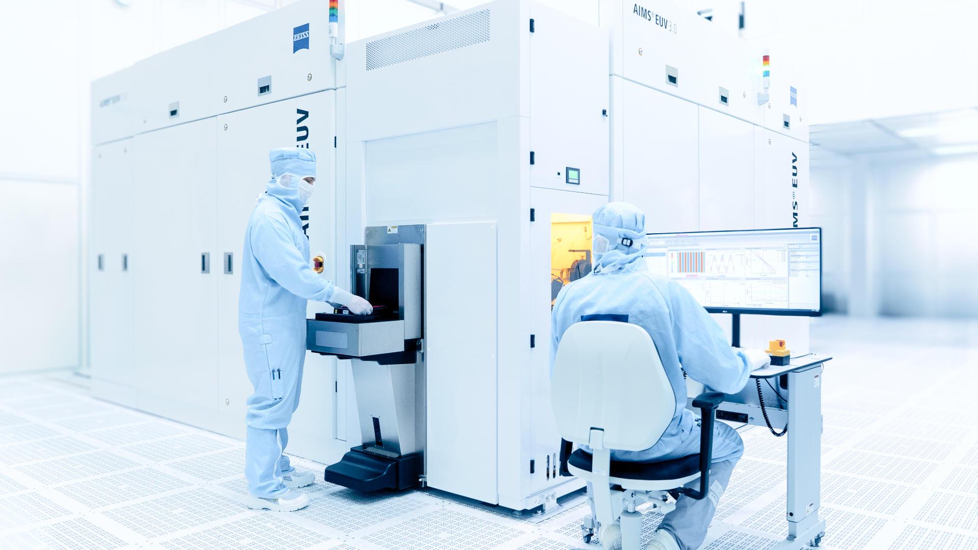
Around 80 percent of all microchips worldwide are manufactured with optics from ZEISS SMT. For more than twenty years, the company in the optical and optoelectronic industry has been producing optics for DUV lithography (DUV stands for “deep ultraviolet light”) at its production site in Wetzlar, the “City of Optics”. “With our lithography optics, we enable chip manufacturers worldwide to produce microchips with nanometer precision,” explains Katrin Ariki, site manager of ZEISS SMT in Wetzlar. Thanks to the constantly growing demand in the market for semiconductor manufacturing equipment, there is a lot to do at ZEISS SMT in Wetzlar - and soon also in the multifunctional factory currently under construction in Wetzlar's Dillfeld, which will expand the production and development capacities by 12,000 square meters. ZEISS SMT is not only adding additional space for optics, coating and assembly, but is also hiring. “In order to advance the technologies of tomorrow, we are looking for skilled workers, especially in the areas of development and production,” says Ariki.

Exchange and networking in a high-tech environment

The company particularly benefits from the existing optics expertise in Hesse as well as the proximity to important research institutions such as the universities in Giessen, Marburg and Frankfurt. The intensive exchange with industry and association representatives is also important in order to master the challenges of the employer market. “Wetzlar and the Central Hesse region are enormously important for us as a technology company. That’s why we feel at home here and want to continue to grow,” explains Ariki.

On Wednesday, March 13, 2024, at 11 a.m., Toralf Gruner, systems engineer at ZEISS SMT, will give a lecture on the topic “Another boost to lithographic resolution – from optical design to AI enabling chips” in the Buderus Arena Wetzlar. Gruner emphasizes: “We are already driving tomorrow’s technologies forward today. In this high-tech, promising environment, we offer exciting job and further training opportunities. We are therefore particularly looking forward to the exchange and networking at the W3+ Fair.”

Portrait of Jeannine Rapp
Press Contact Jeannine Rapp Carl Zeiss SMT GmbH
Portrait of Jeannine Rapp
Press Contact Jeannine Rapp Carl Zeiss SMT GmbH

About ZEISS

ZEISS is an internationally leading technology enterprise operating in the fields of optics and optoelectronics. In the previous fiscal year, the ZEISS Group generated annual revenue totaling 10 billion euros in its four segments Semiconductor Manufacturing Technology, Industrial Quality & Research, Medical Technology and Consumer Markets (status: 30 September 2023).

For its customers, ZEISS develops, produces and distributes highly innovative solutions for industrial metrology and quality assurance, microscopy solutions for the life sciences and materials research, and medical technology solutions for diagnostics and treatment in ophthalmology and microsurgery. The name ZEISS is also synonymous with the world's leading lithography optics, which are used by the chip industry to manufacture semiconductor components. There is global demand for trendsetting ZEISS brand products such as eyeglass lenses, camera lenses and binoculars.

With a portfolio aligned with future growth areas like digitalization, healthcare and Smart Production and a strong brand, ZEISS is shaping the future of technology and constantly advancing the world of optics and related fields with its solutions. The company's significant, sustainable investments in research and development lay the foundation for the success and continued expansion of ZEISS' technology and market leadership. ZEISS invests 15 percent of its revenue in research and development – this high level of expenditure has a long tradition at ZEISS and is also an investment in the future.

With around 43,000 employees, ZEISS is active globally in almost 50 countries with around 30 production sites, 60 sales and service companies and 27 research and development facilities (status: 30 September 2023). Founded in 1846 in Jena, the company is headquartered in Oberkochen, Germany. The Carl Zeiss Foundation, one of the largest foundations in Germany committed to the promotion of science, is the sole owner of the holding company, Carl Zeiss AG.

Further information at www.zeiss.com


Semiconductor Manufacturing Technology

With its product portfolio and expertise, the Semiconductor Manufacturing Technology segment of ZEISS covers a variety of key processes in the production of microchips. Its products include semiconductor manufacturing optics – notably lithography optics – as well as photomask systems and process control solutions for semiconductor manufacturing. Thanks to ZEISS technology, microchips are becoming increasingly smaller, more powerful, more energy-efficient and more affordable. The electronic applications of these ongoing enhancements enable global progress in many disciplines such as technology, electronics, communication, entertainment, mobility and energy. Semiconductor Manufacturing Technology is headquartered in Oberkochen. Other sites include Jena, Rossdorf, Wetzlar and Aachen in Germany, as well as Bar Lev (Israel) and Dublin, CA and Danvers, MA (USA).

Further information