Press release

ZEISS SMT opens new cleanrooms at Rossdorf site

17 September 2025 · 4 min read
  • The segment ZEISS Semiconductor Manufacturing Technology (SMT) has expanded its research and development site in Rossdorf
  • 300 square meters of cleanroom space have been added.
  • Hesse’s Prime Minister Boris Rhein: "A strong signal for our economic location“.
Rossdorf, Germany | 17 September 2025 | ZEISS Semiconductor Manufacturing Technology

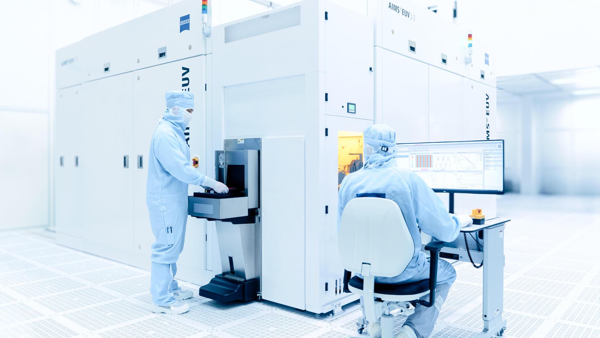
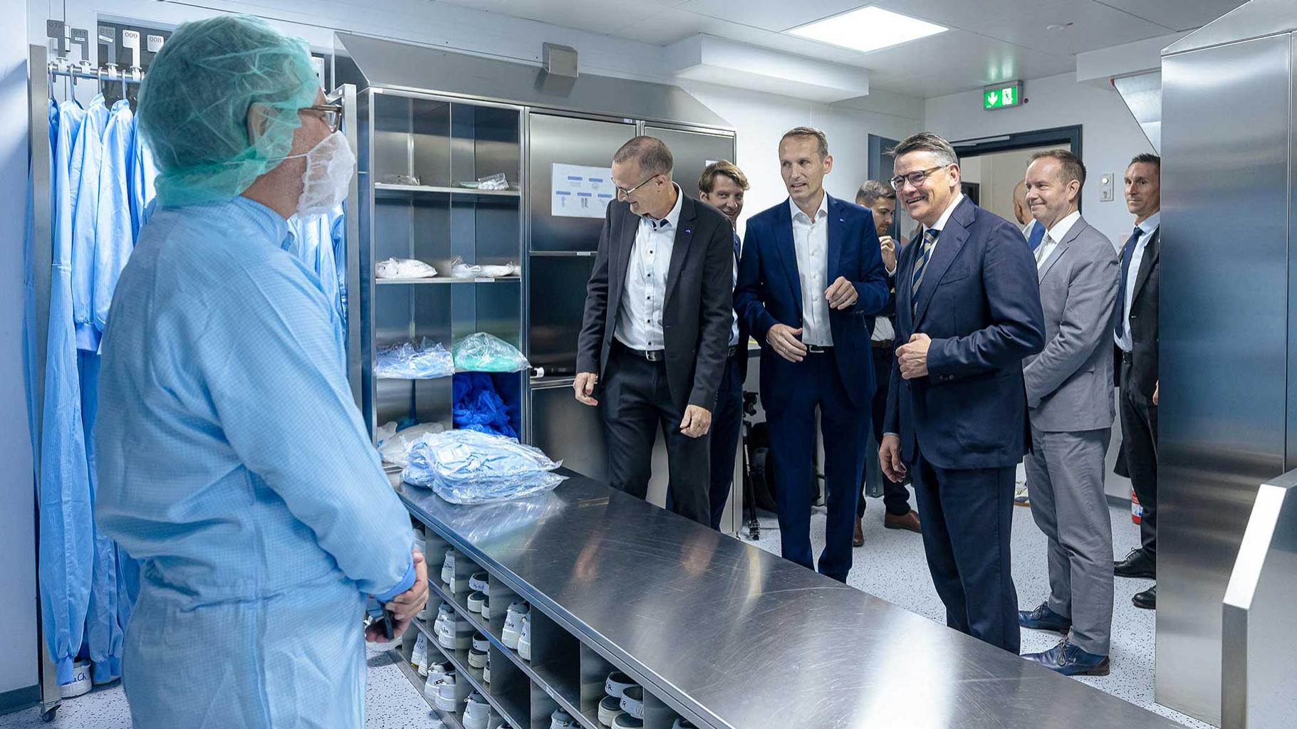
The ZEISS segment Semiconductor Manufacturing Technology (SMT) has put into operation an additional 300 square meters of cleanroom space at its research and development site in Rossdorf, southern Hesse – an increase in area of 80 percent. This strengthens the company's position in a highly specialized area of semiconductor production: the development of high-precision mask repair systems. The measure is part of a larger investment package with a total volume of more than 20 million euros. "The semiconductor industry is of central importance for nearly all future technologies – from autonomous driving to artificial intelligence. That a company like ZEISS is investing in Hesse is a strong signal for our economic location," says Hesse's Prime Minister Boris Rhein. He attended a small opening ceremony on September 17, 2025, in Rossdorf and also took the opportunity to tour the site. Around 280 employees of the strategic business unit ZEISS Semiconductor Mask Solutions (SMS) are employed in Rossdorf.

  • The image shows four people at the ceremonial opening of the new cleanroom space by ZEISS Semiconductor Manufacturing Technology at the Roßdorf site in Hesse. High-precision mask repair systems are developed there.

    Ceremonial opening in Rossdorf: ZEISS Semiconductor Manufacturing Technology (SMT) commissions 300 m² of additional cleanroom space for the development of high-precision mask repair systems – a milestone for the site and the semiconductor industry. The symbolic ribbon cutting was performed by Hesse’s Minister President Boris Rhein, together with Dr. Patrick Villwock, Site and Development Lead in Rossdorf, Dr. Clemens Neuenhahn, Head of ZEISS Semiconductor Mask Solutions (SMS), and Dr. Tilmann Heil, Head of the Field of Business Repair at ZEISS SMS. (from right to left)

  • Opening of the new cleanroom space

    ZEISS SMT expands cleanroom capacity at its Rossdorf site by 300 m² – an increase of 80 percent. The investment of over 20 million euros strengthens the development of high-precision mask repair systems for the semiconductor industry. Hesse’s Minister President Boris Rhein attended the opening ceremony on September 17, 2025.

Room for growth and new tools

With the new cleanrooms, ZEISS SMT not only creates optimal conditions for precision work in the nanometer range – clean, vibration-free, and controlled – but also urgently needed space: the expansion provides room for four additional tools, highly specialized systems that enable the production of defect-free high-end photomasks. "The commissioning is a milestone for our business," says Dr. Clemens Neuenhahn, Head of ZEISS SMS. "We are specifically expanding our research and development capacities to meet the increasing technological complexity in mask repair. ZEISS traditionally invests in research and infrastructure – this is a central prerequisite to remain a technology leader in the future." Rossdorf has been a site of ZEISS SMT since 2005 – at that time, ZEISS acquired NaWoTec GmbH, a spin-off of Deutsche Telekom. "In the past 20 years, our team has grown significantly: in 2015 we were about 80 employees, today around 280. This development shows what is possible with start-up DNA, the backing of a global technology corporation, and the tech ecosystem around Darmstadt," says Dr. Patrick Villwock, development and site manager of ZEISS SMT in Rossdorf.

Location with many advantages

Rossdorf offers several advantages as a location: its position in the Rhine-Main metropolitan region ensures excellent transport connections – with Frankfurt Airport as an international logistics and travel hub. The proximity to the scientific city of Darmstadt, its Technical University, and research institutions is also a crucial plus. ZEISS maintains intensive networks with students and educators and benefits from the proximity to academic talent. Additionally, there is a research cooperation with the ZEISS Innovation Hub @ KIT in Karlsruhe – an interdisciplinary development center at the interface of science and industry.

Precision fort he semiconductor industry

Photomasks serve as optical templates in microchip manufacturing, allowing the finest nanostructures to be exposed on silicon wafers – comparable to an extremely precise slide. Even the smallest defects on these masks can lead to scrap and thus impair the quality and cost-effectiveness of production. The MERiT® systems developed at the Rossdorf site by ZEISS SMT correct such errors contactlessly, using electron beam technology and nanometer precision – without damaging the masks. They help ensure yield in production and guarantee the quality of modern microchips. All major semiconductor manufacturers worldwide use the systems from ZEISS SMT to reliably repair photomasks. As microchips continue to get smaller, more powerful, and more energy-efficient, the demands on repair processes are also increasing. Therefore, the technology in Rossdorf is continuously being further developed.

Portrait of Jeannine Rapp
Press Contact Jeannine Rapp Carl Zeiss SMT GmbH
Portrait of Jeannine Rapp
Press Contact Jeannine Rapp Carl Zeiss SMT GmbH

About ZEISS

ZEISS is an internationally leading technology company in the optics and optoelectronics industry. The ZEISS Group generated annual revenue totaling around 11 billion euros in its four segments Industrial Quality & Research, Medical Technology, Consumer Markets and Semiconductor Manufacturing Technology (updated: 30 September 2024).

For its customers, ZEISS develops, produces, and distributes highly innovative solutions for industrial metrology and quality assurance, microscopy solutions for life sciences and materials research, as well as medical technology solutions for diagnostics and treatment in ophthalmology and microsurgery. The name ZEISS is also synonymous with the world's leading lithography optics, which are used by the chip industry to manufacture semiconductor components. There is global demand for trendsetting ZEISS brand products such as eyeglass lenses, camera lenses and binoculars.

With a portfolio aligned with future growth areas like digitalization, healthcare and Industry 4.0 as well as a strong brand, ZEISS is shaping technological progress and, through its solutions, is extending the horizon of the world of optics and associated areas. ZEISS' significant, sustainable investments in research and development lay the foundation for the success and continued expansion of ZEISS' technology and market leadership. ZEISS invests 14% of its revenue in research and development work – ZEISS has a long tradition of high expenditure in these areas. This also represents the company's investment in the future.

With more than 46,555 employees, ZEISS operates in around 50 countries with more than 60 sales and service sites, 40 research and development sites and 35 production sites worldwide (as of 31 March 2025). The headquarters of the company, which was founded in Jena in 1846, is located in Oberkochen, Germany. The Carl Zeiss Foundation, one of Germany’s largest foundations committed to the promotion of science, is the sole owner of the holding company, Carl Zeiss AG.

Further information at www.zeiss.com


Semiconductor Manufacturing Technology

With its product portfolio and expertise, the Semiconductor Manufacturing Technology segment of ZEISS covers a variety of key processes in the production of microchips. Its products include semiconductor manufacturing optics – notably lithography optics – as well as photomask systems and process control solutions for semiconductor manufacturing. Thanks to ZEISS technology, microchips are becoming increasingly smaller, more powerful, more energy-efficient and more affordable. The electronic applications of these ongoing enhancements enable global progress in many disciplines such as technology, electronics, communication, entertainment, mobility and energy. Semiconductor Manufacturing Technology is headquartered in Oberkochen. Other sites include Jena, Rossdorf, Wetzlar, Aachen and Coswig (Germany), Zurich (Switzerland), as well as Bar Lev (Israel) and Dublin, CA (USA). ZEISS SMT also operates various sales and service sites in the US, China, Taiwan (region), South Korea and Japan.

Press Photos

  • Ribbon cutting in Rossdorf

    Ribbon cutting in Rossdorf: ZEISS Semiconductor Manufacturing Technology opens 300 m² of additional cleanroom space for the development of high-precision mask repair systems – a milestone for the site and the semiconductor industry.

    3 MB
  • Opening of the new cleanroom space

    ZEISS SMT expands cleanroom capacity at its Rossdorf site by 300 m² – an increase of 80 percent. The investment of over 20 million euros strengthens the development of high-precision mask repair systems for the semiconductor industry. Hesse’s Minister President Boris Rhein attended the opening ceremony on September 17, 2025.

    4 MB