Press release

AIMS® EUV 3.0: ZEISS SMT extends global footprint in actinic mask qualification

4 February 2026 · 4 min read
  • New generation AIMS EUV 3.0 production proven actinic mask qualification
  • Serving all leading semiconductor manufacturers
  • Improved performance: Better scanner matching by Digital FlexIllu for Low-NA-EUV and High-NA-EUV lithography on one and the same system
  • Additionally, ZEISS SMT enhanced the first generation AIMS EUV with upgrades keeping customer needs at the core
Oberkochen, Germany | 4 February 2026 | ZEISS Semiconductor Manufacturing Technology

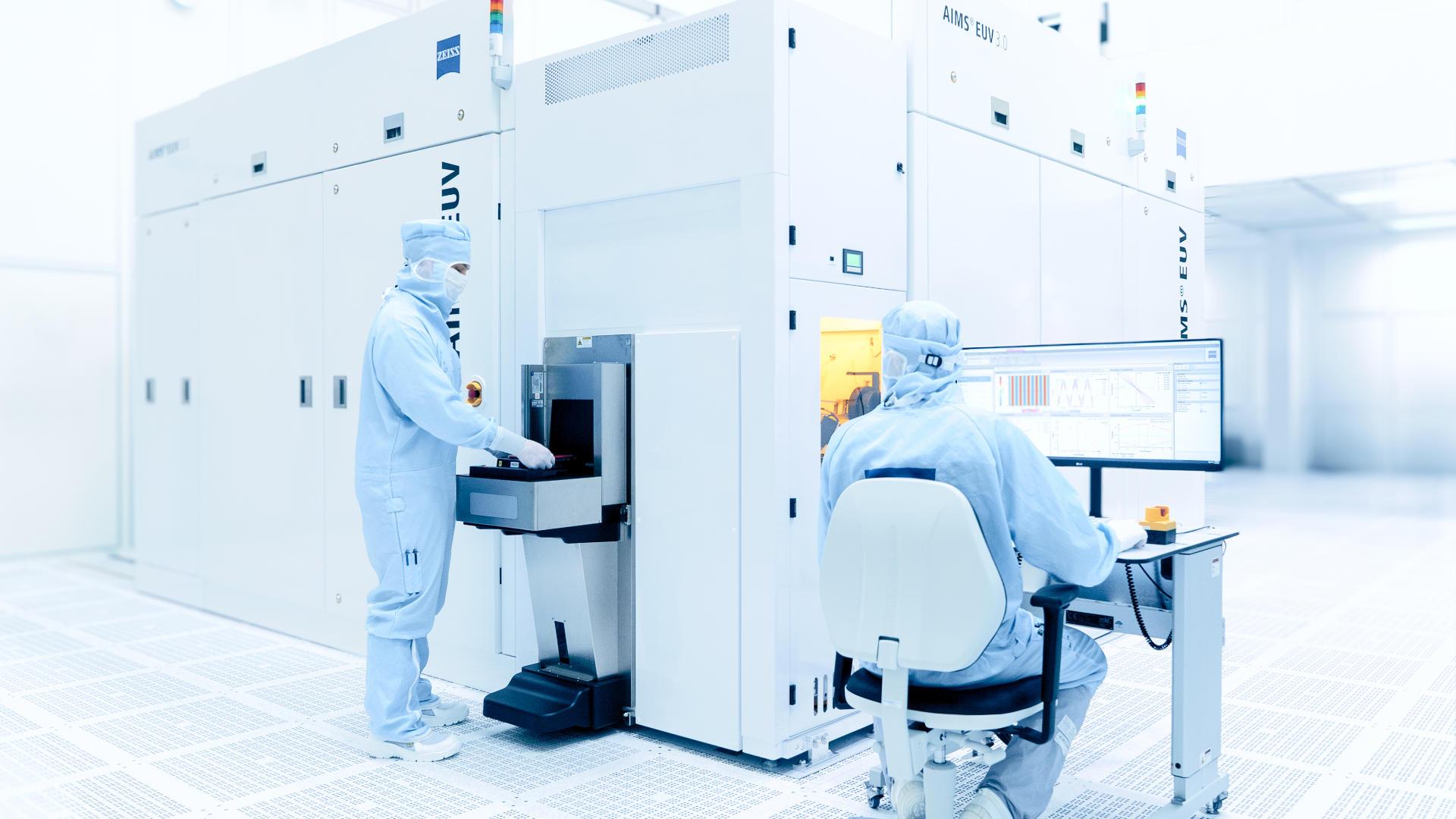
ZEISS Semiconductor Manufacturing Technology (SMT) continues to deploying its new AIMS® EUV 3.0 systems globally at major semiconductor manufacturers. This new generation sets a benchmark in photomask qualification, crucial for performance and functionality of next-generation chips.

A key feature of the AIMS® EUV 3.0 is its improved scanner matching. Thanks to Digital FlexIllu capability, the system can emulate any illumination setting, delivering reliable results on defect printability. The platform supports both Low-NA-EUV and High-NA-EUV lithography, providing future-proof flexibility for chip manufacturers to meet various needs and gain strategic advantages. Compared to its predecessor, the new generation triples mask throughput, increases productivity and offers flexible illumination for customized light settings tailored to specific mask requirements.

Two technicians are standing in a white clean room in front of a Zeiss AIMS EUV machine. They are wearing light blue and white protective garments.

The new generation of production-proven actinic mask qualification systems ZEISS AIMS® EUV 3.0 serves all leading semiconductor manufacturers globally. With improved scanner matching and support for both Low-NA-EUV and High-NA-EUV lithography, it offers future-proof flexibility and sets new industry benchmarks.

New features and innovation roadmap

Highlighting the strategic vision and commitment to innovation, Dr. Clemens Neuenhahn, Head of ZEISS Semiconductor Manufacturing Solutions (SMS), states: "We focus on continuous improvement and innovation, ensuring that our customers have state-of-the-art technology available to succeed in a rapidly evolving industry."

Therefore, ZEISS SMT is rolling out additional features, including Wafer-Level-Critical-Dimension Option, to pilot customers in 2026. These enhancements provide mask manufacturers with expanded options beyond defect verification after repair, empowering them to optimize their processes even further.

ZEISS SMT also remains dedicated to minimizing downtime through ongoing software upgrades, such as the overhead time improvement upgrade, and exploring further enhancements on the roadmap. Neuenhahn underscores the value proposition of the new system: "With AIMS® EUV 3.0, we’re offering a solution that delivers technological excellence and creates value for our customers in everyday production through higher productivity, flexibility, and operational reliability."

Besides the major improvements of the AIMS® EUV 3.0, ZEISS is further enhancing the first generation of AIMS EUV, with upgrades that double throughput, demonstrating its commitment to advancing existing systems and providing increased value to customers.

Portrait of Jeannine Rapp
Press Contact Jeannine Rapp Carl Zeiss SMT GmbH
Portrait of Jeannine Rapp
Press Contact Jeannine Rapp Carl Zeiss SMT GmbH

About ZEISS

ZEISS is an internationally leading technology enterprise operating in the fields of optics and optoelectronics. In the previous fiscal year, the ZEISS Group generated annual revenue totaling almost 12 billion euros in its four segments Semiconductor Manufacturing Technology, Industrial Quality & Research, Medical Technology, and Consumer Markets (September 30, 2025).

For its customers, ZEISS develops, produces, and distributes highly innovative solutions for industrial metrology and quality assurance, microscopy solutions for the life sciences and materials research, and medical technology solutions for diagnostics and treatment in ophthalmology and microsurgery. The name ZEISS is also synonymous with the world's leading lithography optics, which are used by the chip industry to manufacture semiconductor components. There is global demand for trendsetting ZEISS brand products such as eyeglass lenses, camera lenses, and binoculars.

With a portfolio aligned with future growth areas like digitalization, healthcare, and Smart Production and a strong brand, ZEISS is shaping the future of technology and constantly advancing the world of optics and related fields with its solutions. The company's significant, sustainable investments in research and development lay the foundation for the success and continued expansion of ZEISS' technology and market leadership. ZEISS invests 15 percent of its revenue in research and development – this high level of expenditure has a long tradition at ZEISS and is also an investment in the future.

With over 46,600 employees, ZEISS is active globally in around 50 countries with more than 60 sales and service locations, around 40 research and development facilities, and 30 production facilities worldwide (September 30, 2025). Founded in 1846 in Jena, the company is headquartered in Oberkochen, Germany. The Carl Zeiss Foundation, one of the largest foundations in Germany committed to the promotion of science, is the sole owner of the holding company, Carl Zeiss AG.

Further information at www.zeiss.com


Semiconductor Manufacturing Technology

With its product portfolio and expertise, the Semiconductor Manufacturing Technology segment of ZEISS covers a variety of key processes in the production of microchips. Its products include semiconductor manufacturing optics – notably lithography optics – as well as photomask systems and process control solutions for semiconductor manufacturing. Thanks to ZEISS technology, microchips are becoming increasingly smaller, more powerful, more energy-efficient and more affordable. The electronic applications of these ongoing enhancements enable global progress in many disciplines such as technology, electronics, communication, entertainment, mobility and energy. Semiconductor Manufacturing Technology is headquartered in Oberkochen. Other sites include Jena, Rossdorf, Wetzlar, Aachen and Coswig (Germany), Zurich (Switzerland), as well as Bar Lev (Israel) and Dublin, CA (USA). ZEISS SMT also operates various sales and service sites in the US, China, Taiwan (region), South Korea and Japan.

Press Photos

  • ZEISS AIMS EUV 3.0

    The new generation of production-proven actinic mask qualification systems ZEISS AIMS® EUV 3.0 serves all leading semiconductor manufacturers globally. With improved scanner matching and support for both Low-NA-EUV and High-NA-EUV lithography, it offers future-proof flexibility and sets new industry benchmarks.

    3 MB