Press release

ZEISS opens Semiconductor Innovation Center in Korea to deepen customer collaboration

10 July 2026
  • New ZEISS Semiconductor Innovation Center in Yongin strengthens the company’s presence in one of the world’s key semiconductor markets, creating a platform to bring ZEISS closer to leading chip and mask manufacturers in Korea
  • The center provides local access to ZEISS solutions for high‑volume wafer production, wafer-level packaging and photomask manufacturing, enabling higher production yield and faster evaluation and qualification in customers’ production environments
  • It serves as a collaboration hub between ZEISS experts and Korea’s semiconductor ecosystem, supporting direct interaction, joint innovation and faster evaluation and qualification along the value chain
Seoul, South Korea  | 10 July 2026 | ZEISS Semiconductor Manufacturing Technology

ZEISS Semiconductor Manufacturing Technology (SMT) has opened a new ZEISS Innovation Center in Yongin, Korea. With this step, ZEISS is expanding its footprint in one of the world’s most important semiconductor markets and strengthening its global network of locations supporting the industry.

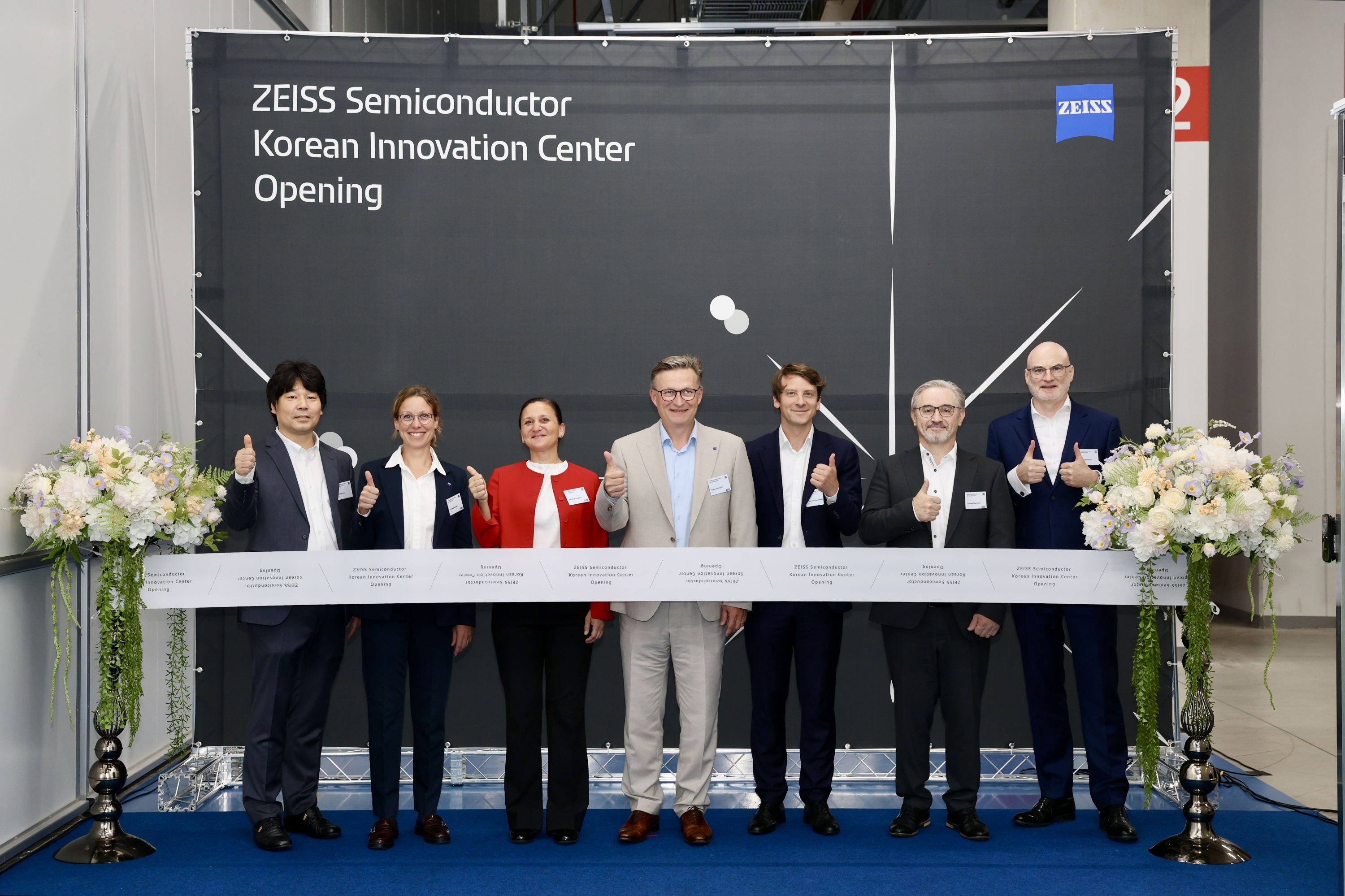
The opening ceremony was attended by Dr. Frank Rohmund, President & CEO of ZEISS Semiconductor Manufacturing Technology and Member of the ZEISS Executive Board, Dr. Thomas Stammler, Chief Technology Officer, Dr. Karoline Piegdon, Head of Semiconductor Fab Solutions (SFS), Dr. Clemens Neuenhahn, Head of Semiconductor Mask Solutions (SMS), and Dr. Jaane Seehusen, who will be appointed Head of ZEISS South Korea as of September 1, 2026, as well as representatives from the Korean semiconductor industry and the German Embassy in Korea, the European Union Chamber of Commerce Korea, and the Korean-German Chamber of Commerce and Industry.

  • Seven ZEISS leaders stand in front of a stage backdrop and ribbon at the ceremonial opening of the Korean Innovation Center.

    Ceremonial opening in Korea: ZEISS Semiconductor Manufacturing Technology opens the Korean Innovation Center – for closer collaboration with local customers. Attending the opening were Jun Seok Lee, Head of ZEISS Semiconductor Manufacturing Technology (SMT) Korea; Dr. Jaane Seehusen, incoming Head of ZEISS Korea as of September 1, 2026; Dr. Karoline Piegdon, Head of Semiconductor Fab Solutions (SFS); Dr. Frank Rohmund, President and CEO of ZEISS Semiconductor Manufacturing Technology and member of the ZEISS Executive Board; Dr. Clemens Neuenhahn, Head of Semiconductor Mask Solutions (SMS); Dr. Thomas Stammler, Chief Technology Officer; and Matthew Wilson, Head of Semiconductor Key Accounts. (from left to right)

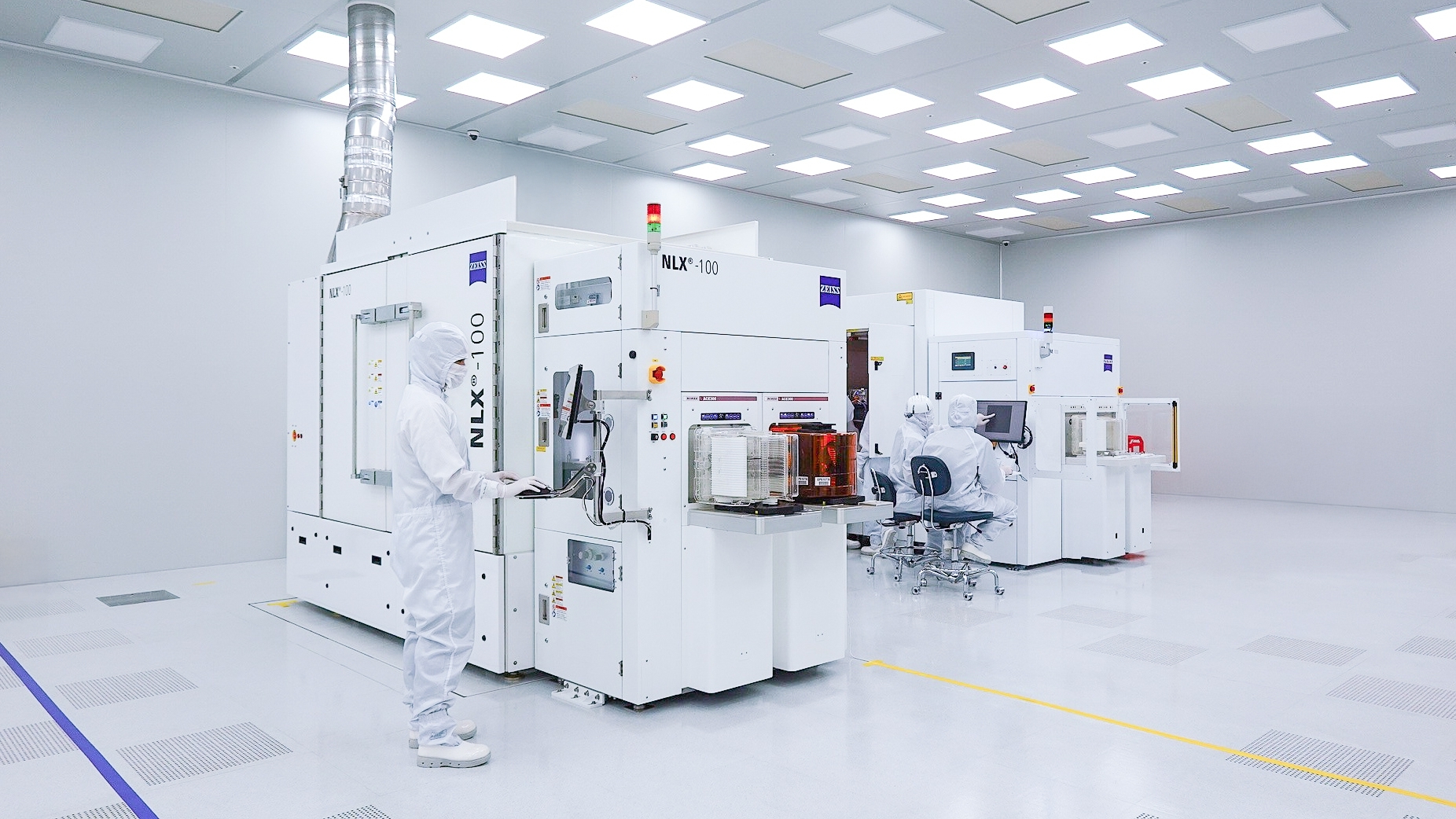
  • Employees in the cleanroom operate ZEISS NLX®‑100 systems for 3D X‑ray metrology and inspection of semiconductor packages.

    Cleanroom at the ZEISS Semiconductor Innovation Center Yongin with NLX®‑100 for 3D X‑ray metrology and inspection.

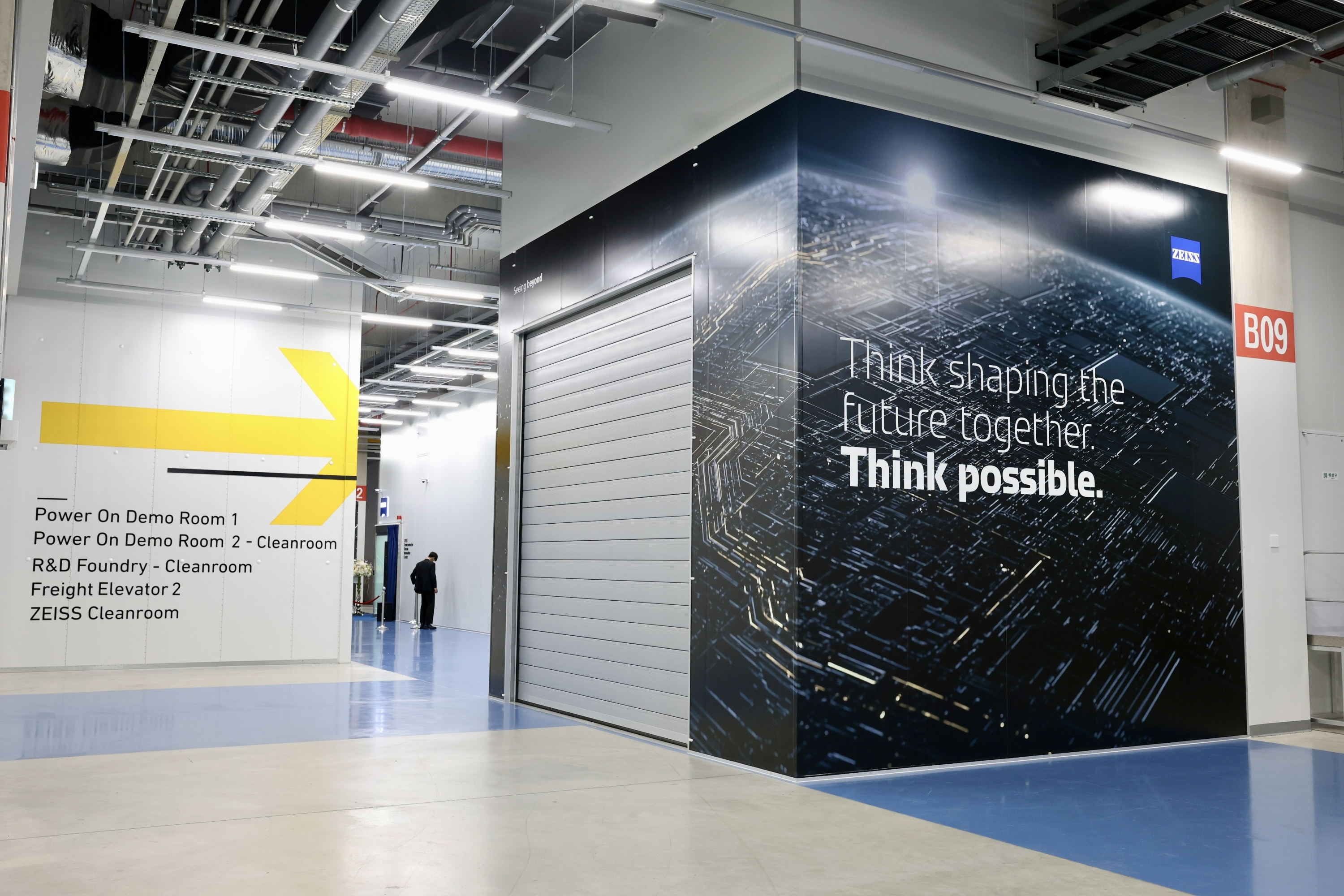
  • View of the entrance area of the ZEISS Semiconductor Korean Innovation Center with a large-scale wall graphic and roller shutter door leading to the demo rooms and cleanrooms.

    View of the entrance of ZEISS Semiconductor Innovation Center in Yongin, Korea.

Local access to ZEISS solutions for high-volume wafer production and advanced packaging

At the new Innovation Center, ZEISS brings together selected systems and solutions from its Semiconductor Mask Solutions and Semiconductor Fab Solutions portfolios. The center is designed to support innovation in high-volume wafer production and advanced packaging applications by leveraging high-precision metrology and inspection, and mask repair technologies.
The systems installed include:

  • NLX®-100: a 3D X-ray metrology & inspection solution that provides high-resolution X-ray diagnostics and data on complex package structures and supports process control, for example in wafer-level and advanced packaging.
  • DUNE®100: enables active wafer shape control with integrated, high precision metrology, allowing fabs to measure and correct global wafer warpage individually for each wafer at every critical step.
  • MeRiT® AE: a future next-generation mask repair technology. It will further extend the capability to repair the most critical and smallest defects on photomasks, with a continued high yield, which is crucial for fine advanced semiconductor processes.

In the future, ZEISS intends to install additional solution equipment in the Korean Innovation Center to strengthen early technical cooperation with customers in Korea.

Local hub for customer collaboration

The ZEISS Semiconductor Innovation Center in Korea functions as a collaborative platform for direct engagement with Korean leading chip manufacturing customers. Dr. Frank Rohmund said, "We are pleased to open our first global Semiconductor Innovation Center in Korea, as one of the key locations for the global chip industry. With this center we are moving ZEISS closer to our customers. We want to be a reliable, long term partner for our customers in Korea and further deepen our collaborations."

By enabling on-site development, process optimization and faster qualification for high-volume production environments, the center helps to accelerate the transition from research and development to customer adoption.

Dr. Jaane Seehusen, future Head of ZEISS Korea, states: “The Innovation Center in Yongin is an important step in our strategy to strengthen customer interaction in the semiconductor industry and additionally ZEISS‘s overall presence in Korea.”
Portrait of Jeannine Rapp
Press Contact Jeannine Rapp Carl Zeiss SMT GmbH
Portrait of Jeannine Rapp
Press Contact Jeannine Rapp Carl Zeiss SMT GmbH
Press Contact Jay Kim ZEISS Korea

About ZEISS

ZEISS is an internationally leading technology enterprise operating in the fields of optics and optoelectronics. In the previous fiscal year, the ZEISS Group generated annual revenue totaling almost 12 billion euros in its four segments Semiconductor Manufacturing Technology, Industrial Quality & Research, Medical Technology, and Consumer Markets (September 30, 2025).

For its customers, ZEISS develops, produces, and distributes highly innovative solutions for industrial metrology and quality assurance, microscopy solutions for the life sciences and materials research, and medical technology solutions for diagnostics and treatment in ophthalmology and microsurgery. The name ZEISS is also synonymous with the world's leading lithography optics, which are used by the chip industry to manufacture semiconductor components. There is global demand for trendsetting ZEISS brand products such as eyeglass lenses, camera lenses, and binoculars.

With a portfolio aligned with future growth areas like digitalization, healthcare, and Smart Production and a strong brand, ZEISS is shaping the future of technology and constantly advancing the world of optics and related fields with its solutions. The company's significant, sustainable investments in research and development lay the foundation for the success and continued expansion of ZEISS' technology and market leadership. ZEISS invests 15 percent of its revenue in research and development – this high level of expenditure has a long tradition at ZEISS and is also an investment in the future.

With over 46,600 employees, ZEISS is active globally in around 50 countries with more than 60 sales and service locations, around 40 research and development facilities, and 30 production facilities worldwide (September 30, 2025). Founded in 1846 in Jena, the company is headquartered in Oberkochen, Germany. The Carl Zeiss Foundation, one of the largest foundations in Germany committed to the promotion of science, is the sole owner of the holding company, Carl Zeiss AG.

Further information at www.zeiss.com


ZEISS Semiconductor Manufacturing Technology

With its product portfolio and expertise, the Semiconductor Manufacturing Technology segment of ZEISS covers a variety of key processes in the production of microchips. Its products include semiconductor manufacturing optics – notably lithography optics – as well as photomask systems and solutions for leading-edge microchip and chiplet production. Thanks to ZEISS technology, microchips are becoming increasingly smaller, more powerful, more energy-efficient and more affordable. The electronic applications of these ongoing enhancements enable global progress in many disciplines such as technology, electronics, communication, entertainment, mobility and energy. Semiconductor Manufacturing Technology is headquartered in Oberkochen. Other sites include Jena, Rossdorf, Wetzlar, Aachen and Coswig (Germany), Zurich (Switzerland), as well as Bar Lev (Israel) and Dublin, CA (USA). ZEISS SMT also operates various sales and service sites in the US, China, Taiwan (region), South Korea and Japan.

Press Photos

  • Opening of the ZEISS Semiconductor Korean Innovation Center

    Ceremonial opening in Korea: ZEISS Semiconductor Manufacturing Technology opens the Korean Innovation Center – for closer collaboration with local customers. Attending the opening were Jun Seok Lee, Head of ZEISS Semiconductor Manufacturing Technology (SMT) Korea; Dr. Jaane Seehusen, incoming Head of ZEISS Korea as of September 1, 2026; Dr. Karoline Piegdon, Head of Semiconductor Fab Solutions (SFS); Dr. Frank Rohmund, President and CEO of ZEISS Semiconductor Manufacturing Technology and member of the ZEISS Executive Board; Dr. Clemens Neuenhahn, Head of Semiconductor Mask Solutions (SMS); Dr. Thomas Stammler, Chief Technology Officer; and Matthew Wilson, Head of Semiconductor Key Accounts. (from left to right)

    4 MB
  • Entrance area of the ZEISS Semiconductor Innovation Center

    View of the entrance of the ZEISS Semiconductor Innovation Center in Yongin, Korea.

    3 MB
  • ZEISS Innovation Center Korea

    Cleanroom at the ZEISS Semiconductor Innovation Center Yongin with NLX®‑100 for 3D X‑ray metrology and inspection.

    1 MB