ZEISS at SEMICON Taiwan 2026
- At SEMICON Taiwan 2026, ZEISS SMT positions as a technology partner for the next generation of semiconductor production.
- The focus will be on advanced packaging as well as metrology and inspection solutions that enable greater precision and stability in complex production processes.
- With the trade show ZEISS SMT underscores the importance of staying close to customers in a leading semiconductor market with strong production capabilities and a dense innovation ecosystem.
ZEISS Semiconductor Manufacturing Technology (SMT) will be represented at SEMICON Taiwan in Taipei from September 2 to 4, 2026. The trade show presence will focus on advanced packaging and technologies that support customers as process complexity rises, tolerances become tighter, and requirements for yield and stability increase.
ZEISS SMT enables lithography manufacturing with its strategic partner ASML by developing its optical systems. Additionally, with solutions from its Semiconductor Mask Solutions and Semiconductor Fab Solutions portfolios, ZEISS SMT helps chip manufacturers control complex production steps more reliably: from technologies for highly precise photomasks, which serve as templates for chip structures in lithography, to the inspection and metrology of fine structures on wafers, and the control of deformations.
Taiwan is one of the world’s leading semiconductor hubs and continues to gain strategic importance as demand grows for high-performance semiconductors used in artificial intelligence applications. The dense ecosystem of foundries, fabless companies, memory manufacturers, packaging providers, research institutions, mask shops and suppliers accelerates innovation and technology adoption across the entire value chain.


Precision and process control for advanced packaging
Advanced packaging is becoming a strategic priority because chip manufacturers need to enable higher performance, lower energy consumption, and more functions in a smaller space. At the same time, requirements for measurement accuracy, defect detection, and process stability are increasing as chip structures become smaller, denser, and more three-dimensional.
"Taiwan is a key site for the global semiconductor industry and a market where new requirements for performance, integration, and production precision become visible particularly early. For ZEISS SMT, SEMICON Taiwan is therefore an important platform for deepening direct exchange with customers and partners. This proximity helps us better understand technological developments and align solutions with the requirements of the next chip generation," says Dr. Frank Rohmund, President and CEO of ZEISS Semiconductor Manufacturing Technology and Member of the ZEISS Executive Board.
"Advanced packaging significantly increases the requirements for process control and defect detection. Our solutions help customers make complex structures on the wafer or in the package visible, keep processes stable, and transfer new technologies into reliable production more quickly," says Dr. Karoline Piegdon, Head of Semiconductor Fab Solutions at ZEISS SMT.
Greater control for complex chip structures
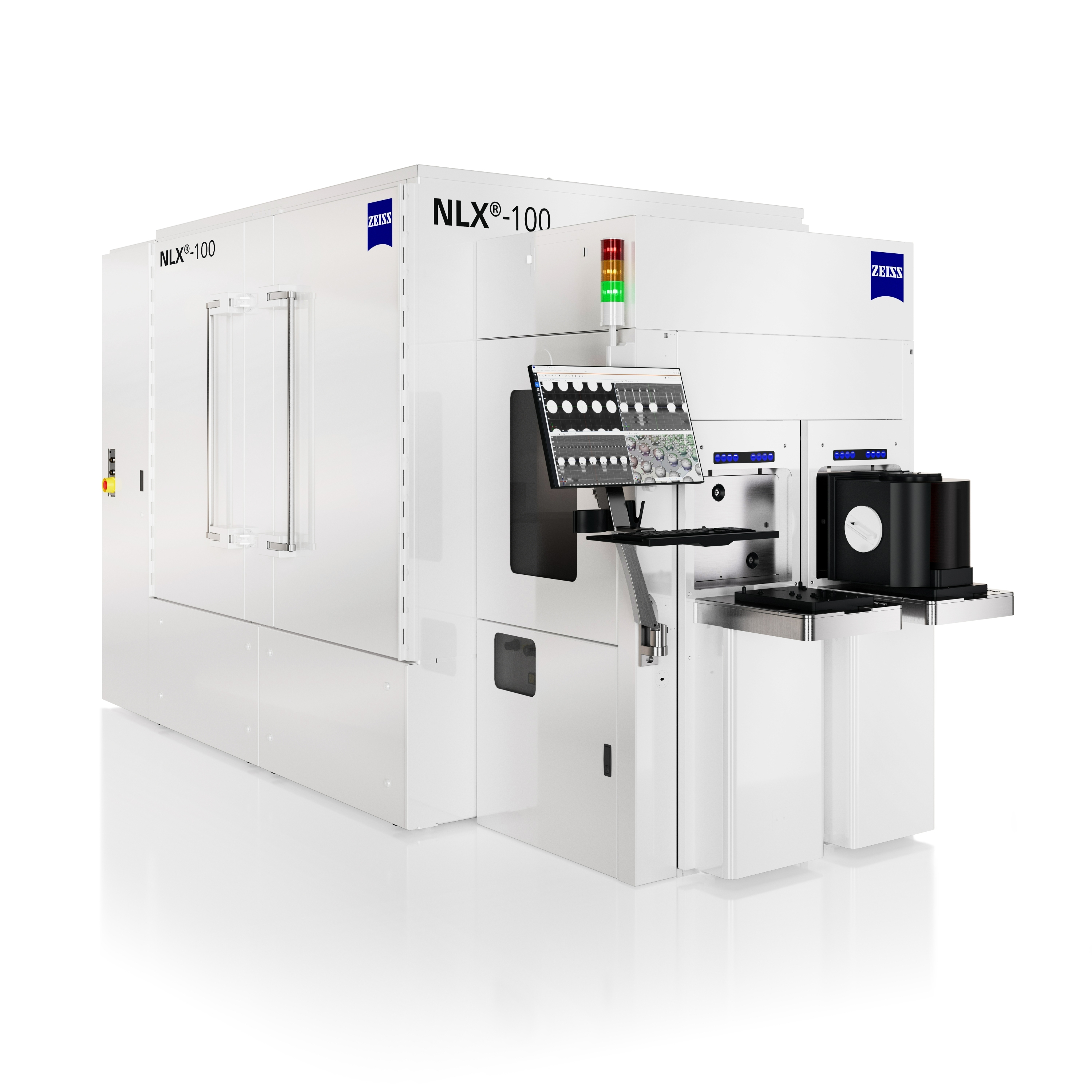
ZEISS NLX shows what this kind of process control can look like. The system makes the internal structures of modern chip packages visible without destroying them. This allows chip manufacturers to inspect connections between stacked dies, for example, and detect potential defects at an early stage. Designed for 300 mm wafers, ZEISS NLX supports both process development and use in volume production.
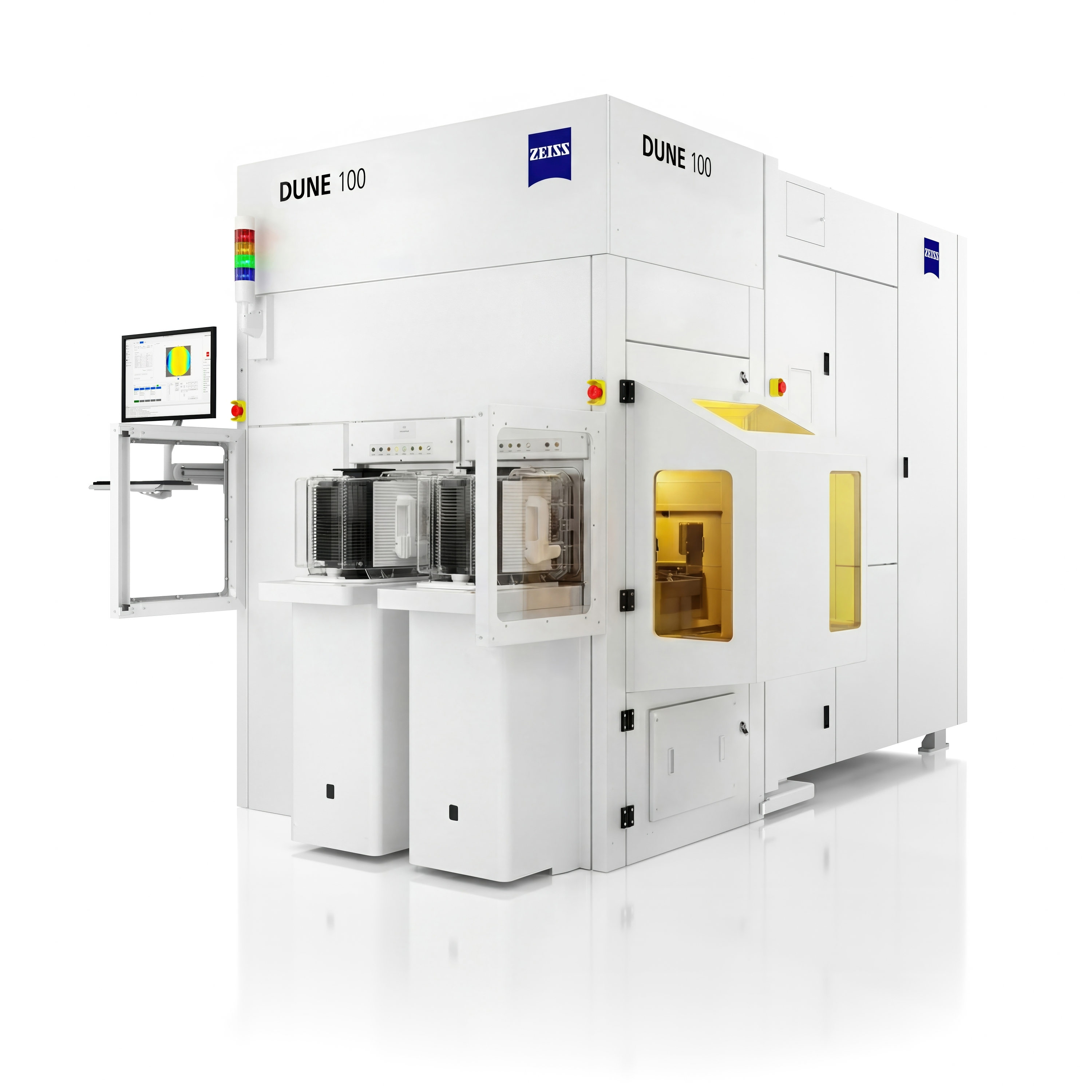
ZEISS DUNE helps to control wafer bow in a targeted way. The system measures the wafer’s topography and can correct it individually. This is especially important in complex production steps, for example, to avoid yield losses during further processing or when preparing for bonding.
In addition, ZEISS SMT is strengthening local availability of this technology in Taiwan: starting at the end of September, installation of a ZEISS DUNE 100 system will begin in Taiwan to enable customers to discuss specific applications directly on site.
Broad range of mask solutions enables flawless production of high-end photomasks
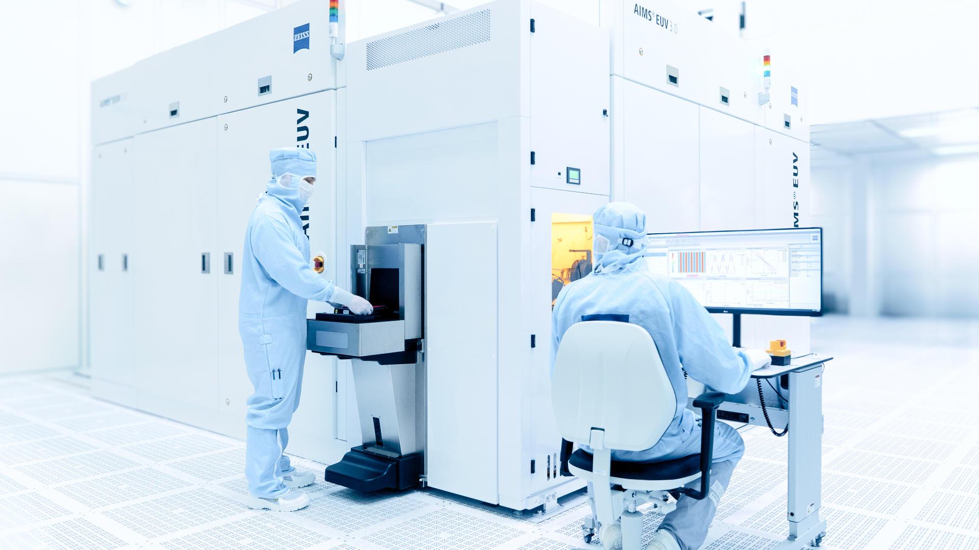
ZEISS SMT's Semiconductor Mask Solutions strategic business unit (SMS) provides leading solutions for reliably manufacturing high-quality photomasks to the market. One example of this is the new AIMS® EUV 3.0 system, which is deployed globally at major semiconductor manufacturers. This new generation sets a benchmark in photomask qualification, crucial for performance and functionality of next-generation chips.
For ZEISS SMS, Taiwan is a very important market as many technology requirements for top notch photomask production become visible in Taiwan at an early stage. "We focus on continuous improvement and innovation, ensuring that our customers have state-of-the-art technology available to succeed in a rapidly evolving industry,” says Dr. Clemens Neuenhahn, Head of Semiconductor Mask Solutions at ZEISS SMT. "Close exchange with local customers and partners helps us understand where the industry is heading and align our mask solutions with the requirements of next-generation chip manufacturing."
Customer proximity in Asia
With its presence at SEMICON Taiwan, ZEISS SMT is building on its efforts to stay close to customers in key Asian semiconductor markets. In July 2026, ZEISS SMT opened a Semiconductor Innovation Center in Yongin, Korea, to deepen collaboration with customers and provide local access to selected solutions for high-volume wafer production, wafer-level packaging, and photomask production. The center supports on-site development, process optimization, and faster qualification for high-volume production environments.
For Taiwan as well, ZEISS SMT plans to further expand access to technologies and application-focused exchange on site in the future.