Advanced packaging: turning complexity into innovation
10 November 20264 minread
High-performance computing, data-intensive applications, and artificial intelligence in particular demand increasingly powerful semiconductor devices. Alongside advances in lithography, advanced packaging plays a major role in system performance. It brings different chips, such as logic and memory chips, together in a single package, placing them close to one another or stacking them vertically and connecting them. Precise coordination between the individual chips enables faster, more efficient data flows that consume less energy across the entire chip architecture.
System integration: a second driver of innovation
For decades, progress in the semiconductor industry was measured by the number of transistors on a chip. High-NA-EUV lithography, for example, enables more computing power in ever-smaller areas, helping extend Moore’s law. Yet miniaturization alone is increasingly reaching its economic and physical limits. Alongside continued scaling, system integration is therefore becoming more important. Advanced packaging combines different semiconductor modules into a cohesive, highly precise chip architecture. Performance gains no longer come solely from advances at the transistor level, but increasingly from the close interaction of different types of memory, chiplets, and technology nodes. Alongside lithography, system integration is becoming a second driver of innovation.
Lower data transfer costs per bit
Short connections between the individual components in a package allow signals to travel faster, minimizing latency and energy consumption. But advanced packaging also presents new challenges for the semiconductor industry: chip architectures become significantly more complex. Different materials, manufacturing steps, and chiplets need to work together with high precision. As components move closer together and the number of interconnections grows, tolerances for positioning, alignment, and electrical connections become tighter. Even small deviations can affect the functionality of the entire package. Hidden defects, material stresses, and wafer warpage therefore need to be detected, controlled, and, where necessary, corrected in advance. Ultimately, the bonding process itself determines functionality, scalability, and yield – the percentage of functional devices produced.
Manufacturing complex chip architectures reliably
This brings a key question into focus for the semiconductor industry: How can these highly complex chip architectures be manufactured consistently, reproducibly, and cost-effectively? Variations that remain within the process window for less complex architectures can affect functionality and failure rates as integration density increases. These include warpage, hidden defects, shifts between individual layers, and bonding precision. As these factors become more critical, so do metrology, inspection, and process control. This is where the ZEISS Semiconductor Manufacturing Technology (SMT) segment comes in. Precision, defect detection, process expertise, and manufacturing stability are core strengths of ZEISS SMT, providing an important foundation for advanced packaging applications. Drawing on decades of development in semiconductor manufacturing, particularly in lithography and metrology, ZEISS SMT offers proven solutions to key challenges in advanced packaging manufacturing.
ZEISS SMT: before, during, and after bonding
Four examples illustrate how ZEISS SMT technologies address key requirements in the growing advanced packaging market:
Wafers can become significantly warped over the course of numerous processing steps. For precise wafer-to-wafer bonding, however, the structures on the wafers must align exactly. ZEISS DUNE creates the conditions needed to achieve this: the system measures wafer warpage, calculates a customized correction pattern, and precisely adjusts the overall wafer shape. A follow-up measurement verifies the result.
ASML
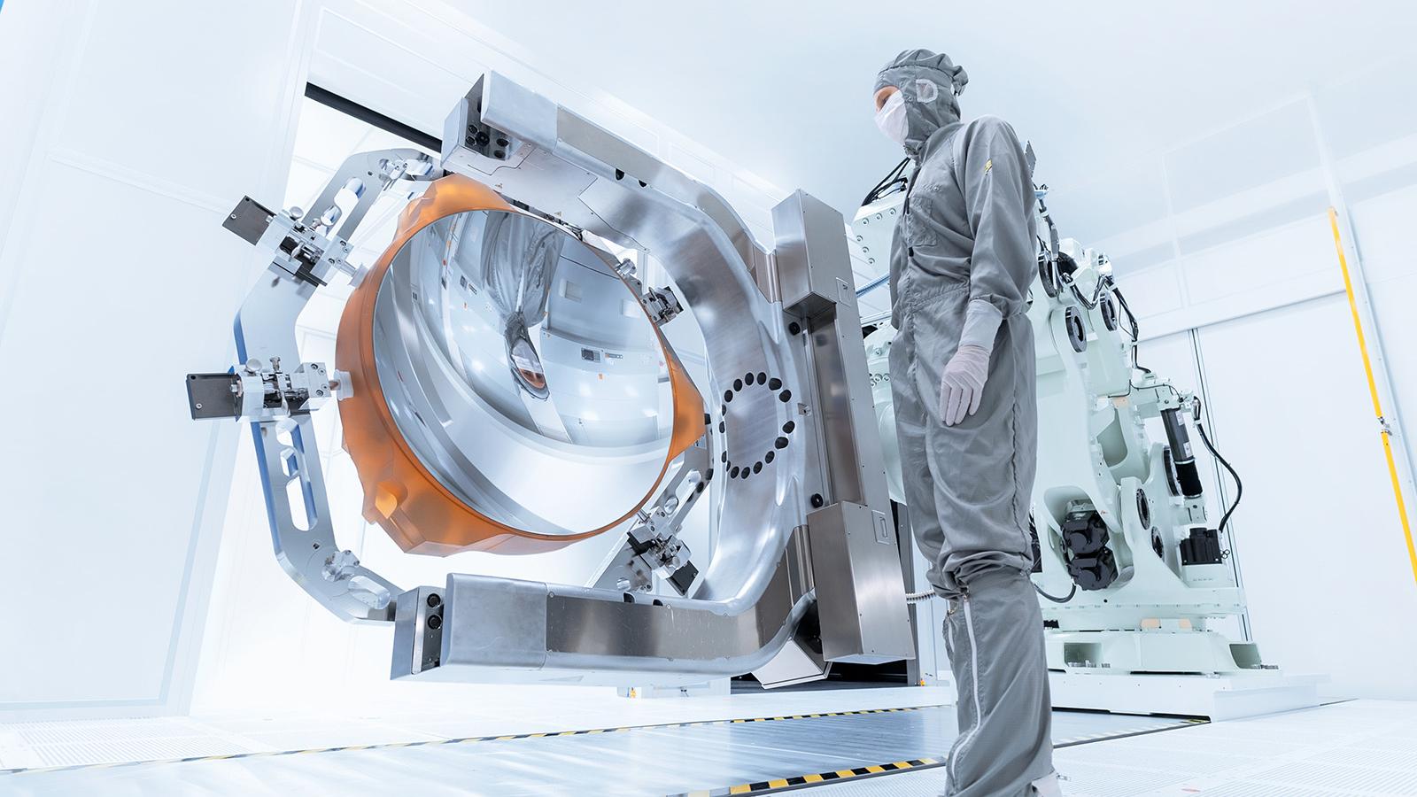
Some bonding processes use interposers, which carry logic, memory, and other chiplets. Manufacturing interposers does not require extremely high lithographic resolution, but it does place specific demands on exposure field size. The XT:260 is tailored to these needs: this deep ultraviolet (DUV) lithography system enables exposure of larger fields, addressing specific requirements in interposer manufacturing.
Third-party Content Blocked
The video player is blocked due to your cookie preferences. To change the settings and play the video, please click the button below and consent to use of "Functional" tracking technologies.
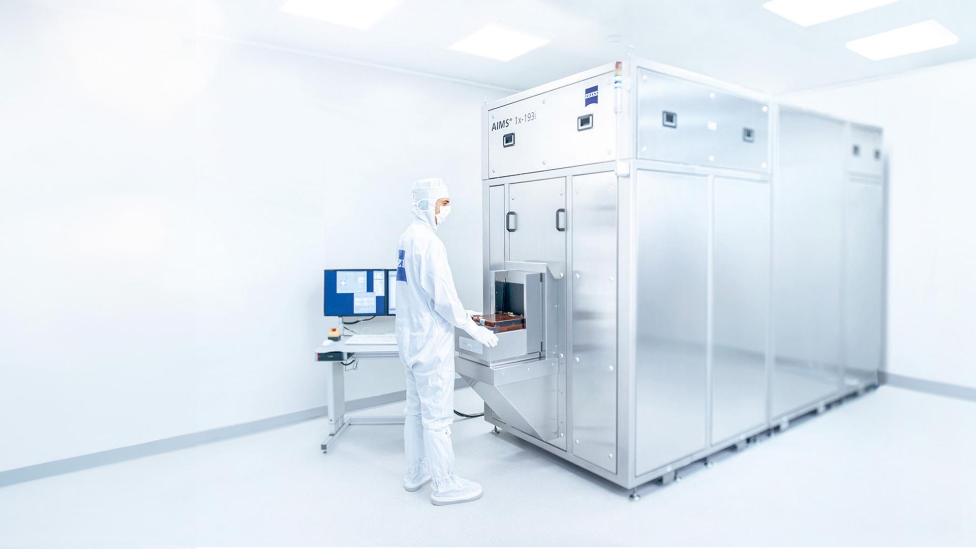
After bonding, critical structures are located inside the package and are no longer accessible to optical inspection methods. The ZEISS NLX inline X-ray microscope enables nondestructive inspection of three-dimensional structures inside thin, large-area samples.
Wafer 3D Metrology and Defect Review is used for inline 3D characterization, 3D metrology, and defect analysis. Using electron optics, the system captures three-dimensional structures in semiconductor devices down to the nanometer scale. This reduces the time needed for analyses that previously took several days.
Advanced packaging unlocks additional performance through the highly precise integration of different components within a package. The key is to turn this potential into stable, cost-effective manufacturing processes with high yields. At ZEISS, we support our customers by contributing to their success with new production, metrology, and defect detection solutions.
From measurement to a stable process
Advanced packaging illustrates how the core capabilities needed in chip manufacturing are changing. In future value chains, advancing individual technologies will no longer be enough. Instead, the challenge will be to bring a wide range of technologies together reliably and integrate them into stable, cost-effective manufacturing processes. With deep expertise in process control, a strong command of complex integration requirements, and a broad product portfolio, ZEISS SMT is a technology partner playing a leading role in shaping the semiconductor industry.
Author
Dr. Michael Hentschel
Head of Field of Business Advanced Packaging