ZEISS Sigma FE-SEM for High-Quality Imaging & Advanced Analytical Microscopy
The ZEISS Sigma family combines field emission scanning electron microscope (FE-SEM) technology with an excellent user experience. Structure your imaging and analysis routines and increase productivity. Study new materials, particles for quality inspection or biological or geological specimens. Make no compromises in high resolution imaging – go to low voltages and benefit from enhanced resolution and contrast at 1 kV or below. Execute advanced analytical microscopy using best-in-class EDS geometry and get analytical data at twice the speed and with more precision.
With the Sigma family you are entering the world of high-end nano-analysis.


Sigma 360
The Core Facility’s Choice. Intuitive Acquisition.- Be guided expertly from setup to AI-based results. Discover an intuitive imaging workflow.
- See the difference at 1 kV and below. Achieve enhanced resolution and optimized contrast.
- Perform VP imaging at the extremes to achieve excellent results on non-conductors.
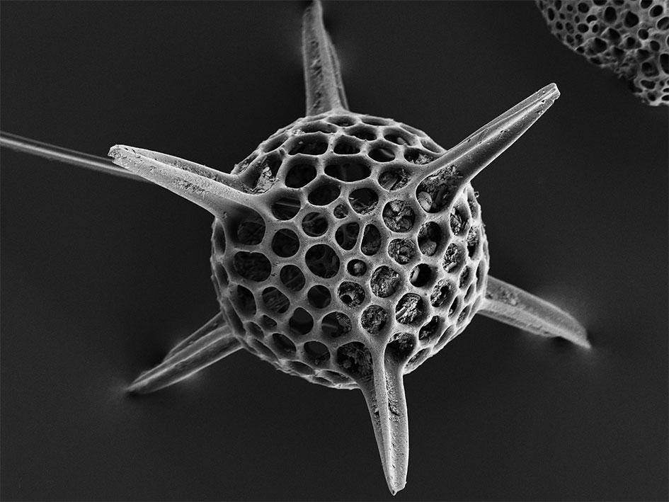
Caption: Polystyrene, imaged with NanoVP lite mode.


Sigma 560
High Throughput Analytics. Automated in situ Experiments.- Efficient analytics of real-world samples: SEM-based analyses with speed and versatility.
- Automate your in situ experiments: A fully integrated lab for unattended testing.
- Image challenging samples below 1 kV: Collect comprehensive sample information.


Technology


Schematic cross-section of Gemini optical column with beam booster, Inlens detector and Gemini objective.
Gemini 1 Optics
Gemini 1 optics consists of three elements: objective lens, beam booster, and Inlens detection concept. The objective lens design combines electrostatic and magnetic fields to maximize optical performance while reducing field influences at the sample to a minimum. This enables excellent imaging, even on challenging samples such as magnetic materials. The Inlens detection concept ensures efficient signal detection by detecting secondary (SE) and/or backscattered (BSE) electrons while minimizing time-to-image. The beam booster guarantees small probe sizes and high signal-to-noise ratios.


Schematic cross-section of Gemini 1 optical column with detectors.
Gemini 1 column of Sigma with detectors. 1 Inlens detectors, SE or Duo. 2 ETSE detector, 3 VPSE, 4 C2D, 5 aSTEM, 6 / 7 Advanced EDS detection, & different backscatter detectors, e.g. aBSD1.
Flexible Detection
Sigma features a suite of different detectors. Characterize your samples with the latest detection technology. Get topographical, high resolution information with the ETSE and the Inlens detector for high vacuum mode. Obtain crisp images in variable pressure mode with the VPSE or the C2D detector. Produce high resolution transmission images with the aSTEM detector. Investigate composition and topography with different optional BSE detectors, e.g., the aBSD detector.
, electron beam skirting (green).")
, electron beam skirting (green).")


NanoVP lite Mode
- In NanoVP lite the skirt effect and the beam gas path length (BGPL) are reduced. The reduced skirt leads to an enhanced signal-to-noise ratio in SE and BSE imaging.
- The retractable aBSD with its five annular segments delivers excellent material contrast: it carries the beam sleeve and is fitted under the pole piece during NanoVP lite operation. It provides high throughput and low voltage compositional and topographical contrast imaging and is suitable for VP and HV (high vacuum).


")
")
")
")


")
")
")
")


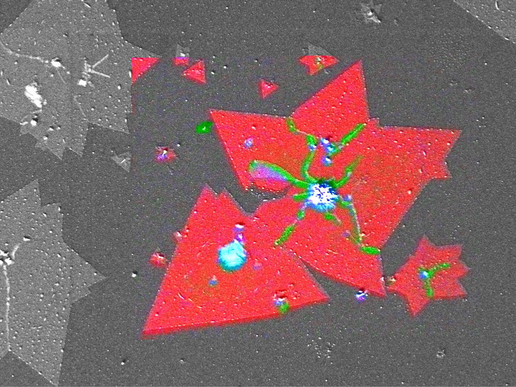


 of garnet-bearing gneiss highlighting geochemical zoning within key minerals.")
 of garnet-bearing gneiss highlighting geochemical zoning within key minerals.")
 of garnet-bearing gneiss highlighting geochemical zoning within key minerals.")
 of garnet-bearing gneiss highlighting geochemical zoning within key minerals.")


Accessories


In Situ Lab for ZEISS FE-SEMs
Link Materials Performance to MicrostructureExtend your ZEISS FE-SEM with an in situ solution for heating and tensile experiments. Benefit from an integrated solution. Investigate materials like metals, alloys, polymers, plastics, composites, and ceramics. Combine a mechanical tensile or compression stage, a heating unit and dedicated high-temperature detectors with analytics. Control all system components from a single PC with a unified software environment that enables unattended automated materials testing.


SmartEDX
Discover Embedded Energy Dispersive X-ray Spectroscopy

Fully Integrated RISE
Benefit from Raman Imaging and Scanning Electron MicroscopyComplement the characterization of your material and add Raman Spectroscopic Imaging (RISE). Get a chemical fingerprint from your sample and extend your Sigma 300 with confocal Raman imaging capability. Recognize molecular and crystallographic information. Perform 3D analysis and correlate SEM imaging, with Raman mapping and EDS data if appropriate. Fully integrated RISE lets you take advantage of both best-in-class SEM and Raman systems.
ZEN core for EM
New SEM Control Software and Entry to Connected MicroscopyBenefit from this software that is more than just a system control: ZEN core is your single, standardized user interface for basic control of ZEISS SEMs and FIB-SEMs. It introduces intuitive, streamlined imaging, and analytics, and lets you perform correlative, multimodal workflows.
Your key features are:
- Easy SEM operation
- Integration of SEM imaging and EDS analysis
- Unique entry point to the ZEN core ecosystem
- Control of basic FIB-SEM workflows including automated multi-site TEM lamella preparation


 and LA-ICP-MS Workflows")
 and LA-ICP-MS Workflows")


")
")