image demonstrates wrinkles and overlapping parts of the MoS2 crystals (green), multilayers (blue) and single layers (red). ZEISS Sigma with RISE.")
 image demonstrates wrinkles and overlapping parts of the MoS2 crystals (green), multilayers (blue) and single layers (red). ZEISS Sigma with RISE.")
Low-D Materials
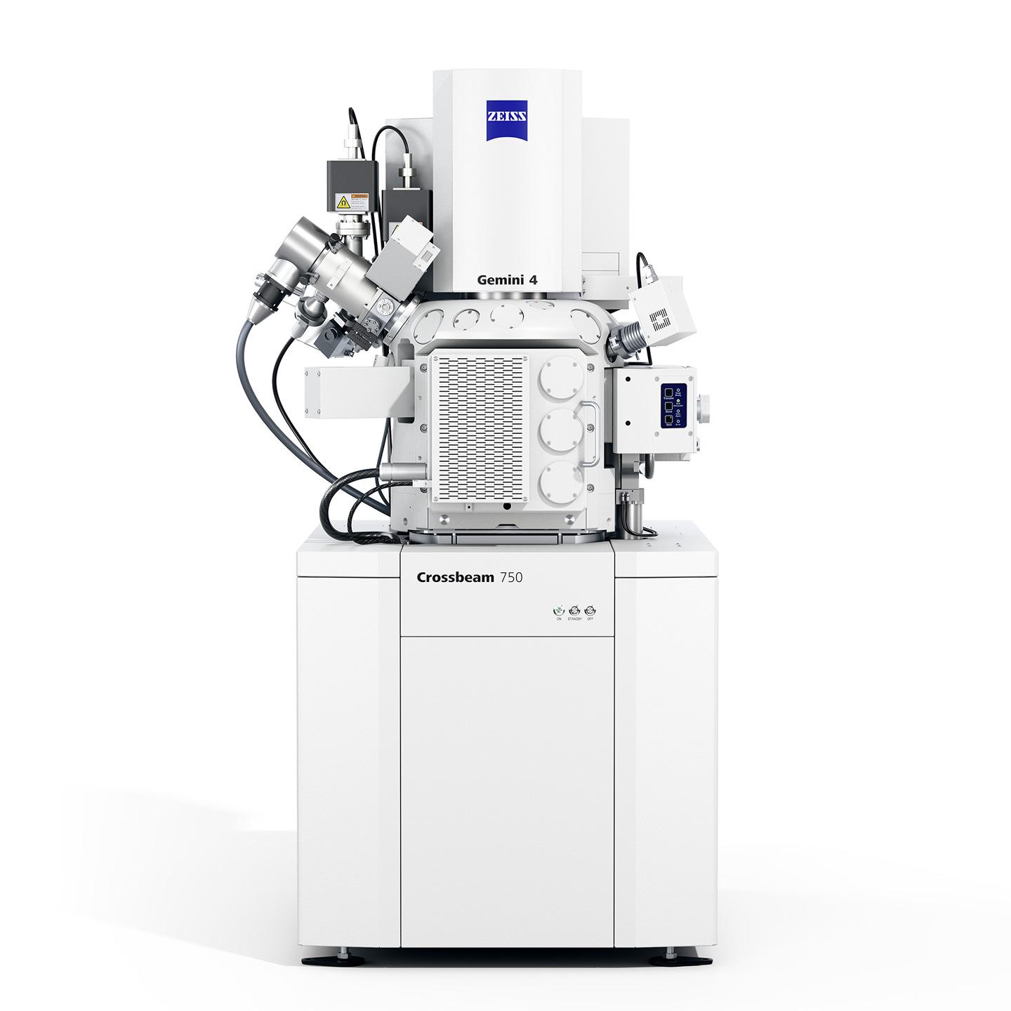
Sub-10 nm Patterning with High Density, High-Resolution Imaging and Analysis of Material SurfacesRecent advances in nanotechnology have pushed the development of FIB-SEM systems that allow higher resolution imaging at lower kV. Excellent low-kV imaging performance is necessary for surface analysis of low-D materials such as MoS2, graphene monolayers, nanowires, nanoparticles, and quantum dots.
The Challenges of Imaging Low-D Materials
Due to quantum confinement effects, these low-D materials demonstrate novel properties not seen in their bulk counterparts. And so high-performance imaging at low-kV isn’t the only requirement. Being able to deposit materials on smaller and smaller length scales (often below 10 - 20 nm) is also necessary. For example, graphene-based devices usually need to have feature sizes below 20 nm to take advantage of quantum confinement. This means you need to pattern ohmic contacts at this length scale before you can test the device.
Another challenge is fabricating structures with a high patterning density. This can be an issue with standard FIB-SEM tools because the beam chemistry limits density due to proximity effects and deposition halos. On the other hand, with sub-10 nm fabrication capabilities, the right instrument can help improve this patterning density.
Finally, creating comprehensive multi-scale, and multimodal 3D images of your region of interest has always been problematic. This is especially true when it comes to low-D materials like nanoparticles. But if done reliably, this kind of analysis can give you valuable information about your sample.
ZEISS Microscopy Offers Powerful Correlative Workflows
ZEISS Microscopy solutions allow you to solve these pressing research challenges in electronics, cybersecurity, and quantum computing. For example, ZEISS MultiSEM - designed for continuous, reliable 24/7 operation - is the world’s fastest SEM instrument. It gives you the acquisition speed of up to 91 parallel electron beams - so you can image samples at the centimeter – scale with nanometer resolution. Click here to learn more.
And the ZEISS Crossbeam FIB-SEM modular platform gives you high-performance SEM imaging at low kV, combined with high FIB sample throughput. But it also allows you to upgrade your FIB-SEM in a modular fashion – such as by installing a laser for massive material ablation - so your microscope keeps pace with your research demands.