Semiconductor and Electronics Research
Making Future Electronic, Cybersecurity, and Quantum Computing Devices a RealityNanotechnology has contributed to many incredible advances across a range of industries, including electronics, cybersecurity, and quantum computing. For years, those advances have been the result of Moore’s law and the consistent miniaturization of transistor sizes - gradually enabling the development of faster, smaller, and more powerful devices.
But fabricating future nanoscale devices is becoming more challenging as Moore’s law approaches its limit. As a result of effects like quantum mechanical tunneling, scientists are unable to make these devices smaller. Instead, by studying different materials and technology - such as stacking transistors vertically (like in 3D NAND) - research can provide the processing power needed for these applications going forward.
Such Devices Cannot Be Characterized Easily
If you’re a scientist involved in electronics, cybersecurity, or quantum computing research, you know how difficult it is to access deeply buried sites in structures like 3D NAND. But with the right workflow involving laser ablation inside a FIB-SEM, you can access these regions quickly and easily, with minimal damage to your sample. 3D tomography inside a FIB-SEM can also help you gain critical information about your sample - information that would typically be unavailable using standard tools.
With cybersecurity, the challenge lies in imaging large processor chips at high resolution and high pixel density. These chips need imaging over massive areas that standard imaging solutions are incapable of handling. The solution is unattended (automated) imaging software and hardware that lets you acquire images of these large areas fast. And when it comes to quantum computing, the challenge is developing (and imaging) sub-10 nm structures in order to create vacancies at very specific locations.
Your Next Step
ZEISS Microscopy solutions allow you to solve these pressing research challenges in electronics, cybersecurity, and quantum computing. For example, ZEISS MultiSEM - designed for continuous, reliable 24/7 operation - is the world’s fastest SEM instrument. It gives you the acquisition speed of up to 91 parallel electron beams - so you can image samples at the centimeter – scale with nanometer resolution.
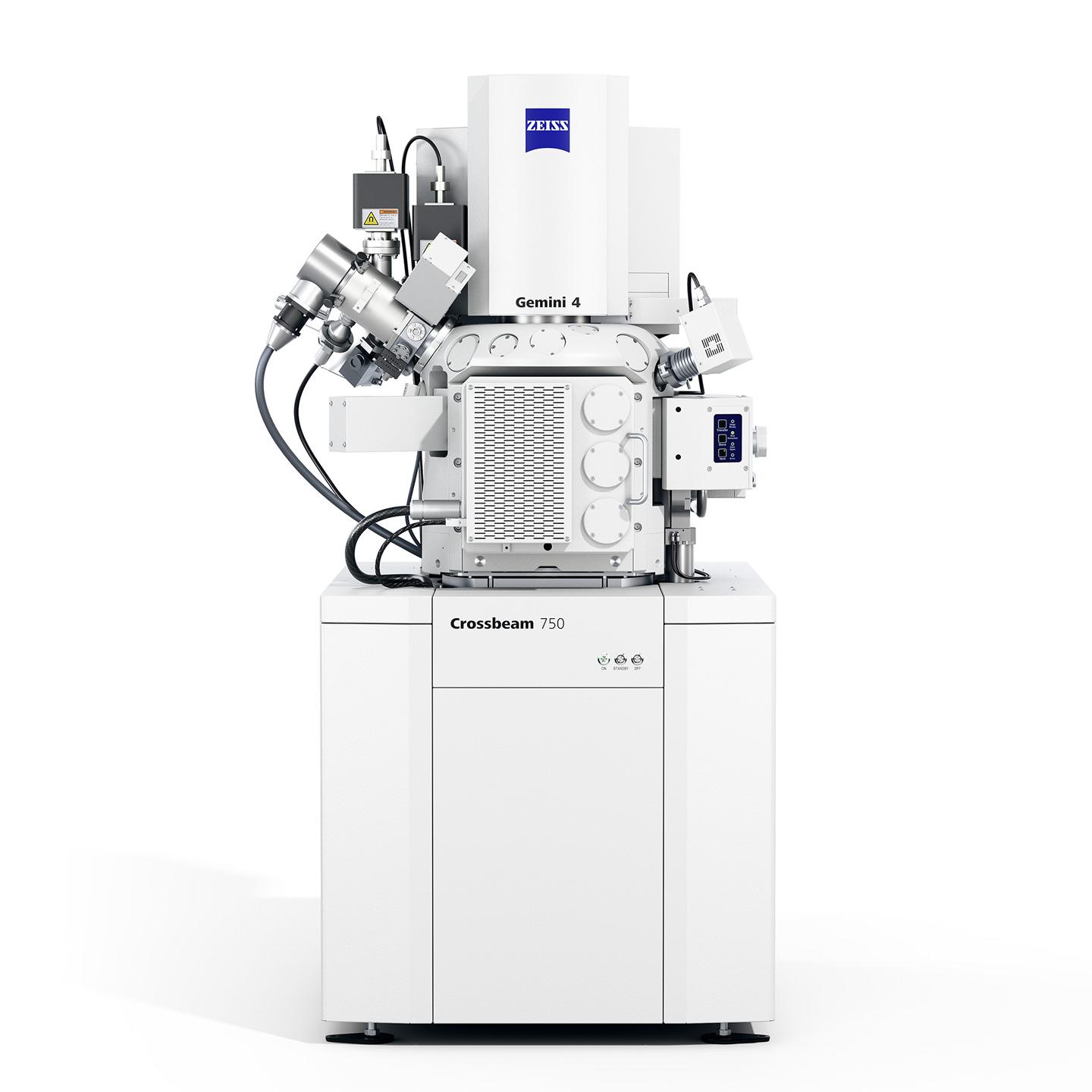
And the ZEISS Crossbeam FIB-SEM modular platform gives you high-performance SEM imaging at low kV, combined with high FIB sample throughput. But it also allows you to upgrade your FIB-SEM in a modular fashion – such as by installing a laser for massive material ablation - so your microscope keeps pace with your research demands.