AI-generated illustration of a researcher using the ZEISS Crossbeam 750 FIB-SEM microscope for imaging and sample preparation.
This image was created by generative AI This image was created by generative AI

ZEISS Crossbeam 750 FIB-SEM

Precision FIB-SEM with live endpoint control for confident, repeatable workflows

ZEISS Crossbeam 750 is engineered for precision and clarity in TEM lamella preparation, 3D tomography, and nanofabrication, meeting the demands of advanced semiconductor and materials research workflows. With Gemini 4 optics and High Dynamic Range (HDR) Mill + SEM, it delivers live, high-resolution imaging during milling, enabling confident endpoint control and repeatable sub-20 nm lamella preparation — even for most complex device architectures and demanding samples.

  • Unmatched imaging performance

    Gemini 4 optics deliver high-resolution visibility during milling.

  • Live see while you mill clarity

    HDR Mill + SEM enables real-time imaging at any sample tilt for confident endpoint control.

  • Precise sub-20 nm lamella preparation

    Achieve ultra-thin lamellae with repeatable accuracy.

  • Reliable repeatability

    Recipe-based workflows and logging ensure consistent results across samples and operators.

ZEISS Crossbeam 750 FIB-SEM microscope system used for high-resolution imaging and precise sample preparation.

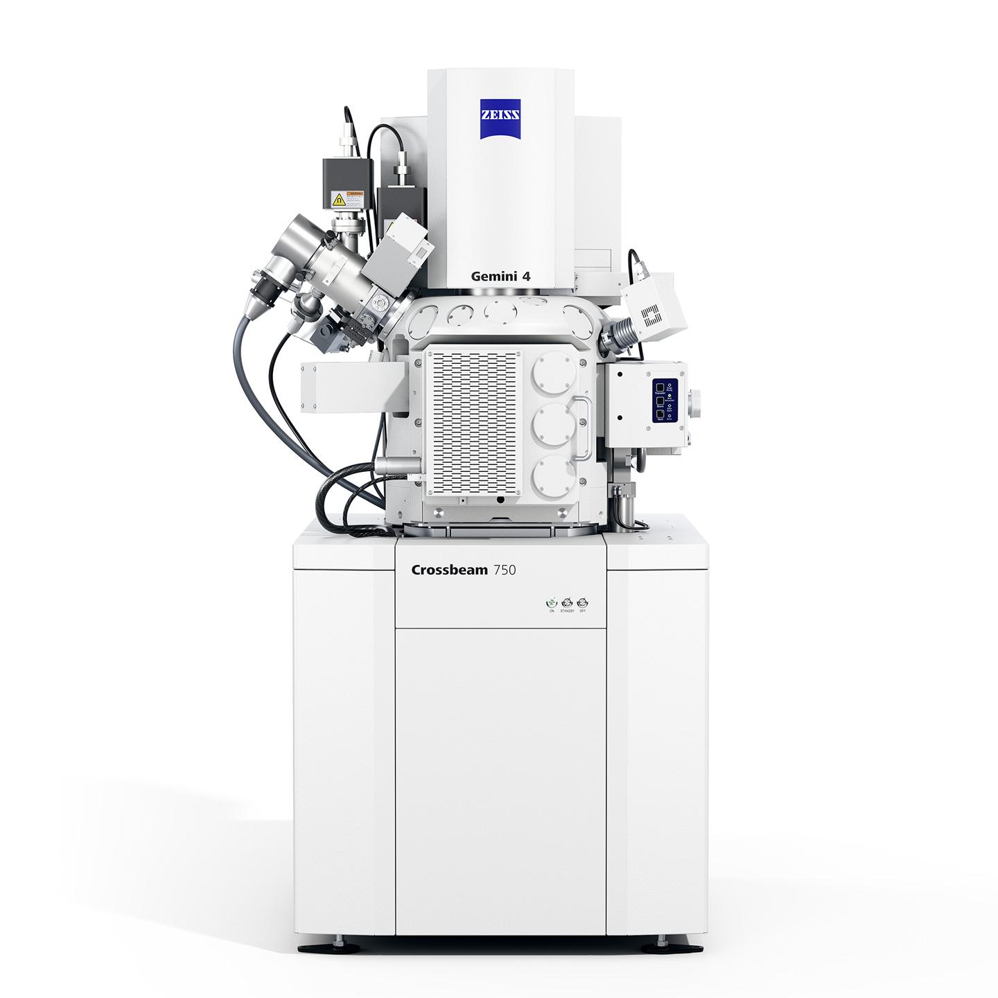
What’s different with Crossbeam 750

Crossbeam 750 introduces a new Gemini 4 objective lens that enhances imaging performance and stability during milling. Combined with HDR Mill + SEM, it delivers live, high-resolution visibility, bringing buried features and delicate interfaces into view as they are exposed. This real-time insight allows users to confidently control endpoints, protect critical structures, and achieve precise sub-20 nm lamella preparation without the need for rework.

Illustration of focused ion beam milling used to prepare thin TEM lamellae for analysis with the ZEISS Crossbeam 750 FIB-SEM.

Key specifications

  • Gemini 4 optics: Field-free objective lens for unmatched imaging performance - also during milling
  • Achieve ultra-thin sub-20 nm lamellae with live FIB and SEM corrections for precision
  • Low-energy FIB finishing minimizes amorphization and preserves fine details
  • Batch processing: Recipe-driven workflows for multi-sample and multi-ROI preparation
Illustration of live SEM monitoring during FIB milling for precise endpoint control and TEM lamella preparation.

Integrated TEM lamella preparation with live imaging control

Crossbeam 750 enables deterministic lamella preparation by combining the Gemini 4 field-free objective lens with continuous SEM imaging during milling. High-resolution imaging lets users monitor interfaces in real-time, precisely align milling planes, and make fine adjustments before critical material is removed. With HDR Mill + SEM, buried features remain clearly visible throughout thinning —supporting confident endpoint control and repeatable sub-20 nm lamella preparation for advanced semiconductor structures such as fins, vias, and gate stacks.

Illustration of ZEISS software interface used with Crossbeam 750 for automated FIB-SEM workflows and 3D image analysis.

Software workflows engineered for Crossbeam 750 precision

ZEISS ZEN core EM software seamlessly integrates acquisition, control, and analysis for the most demanding Crossbeam 750 workflows. ZEN simplifies automated recipes, batch execution, and synchronized SEM/FIB operations. For downstream analysis, ZEISS arivis supports scalable, the ZEISS arivis suite extends capabilities within scalable, AI-driven image analysis. arivis Pro enables flexible multi-dimensional visualization and segmentation pipelines; arivis Hub accelerates and batches high-volume processing; and arivis Cloud provides cloud-based AI model training to automate and scale advanced analysis without coding. Together, these tools enhance nanofabrication, large-area imaging, and correlative workflows with reproducible, top-quality results.

Related applications

SEM micrograph of nanofluidic channels fabricated by focused ion beam milling for micro- and nanofluidics research.

SEM micrograph of nanofluidic channels fabricated by focused ion beam milling for micro- and nanofluidics research.

SEM micrograph of nanofluidic channels fabricated by focused ion beam milling for micro- and nanofluidics research.

Materials Research

  • Clean cross-sections for 3D material characterization using imaging, FIB processing and analytics
  • Precise thinning for high-resolution TEM imaging of complex micro- and nanometer scaled structures
  • Low-damage finishing preserves nanoscale features in materials such as metals, ceramics, and polymers
XY slice from a 3 nm FinFET SRAM 3D tomography dataset showing the Metal 3 layer, imaged with ZEISS Crossbeam 750 FIB-SEM.

XY slice from a 3 nm FinFET SRAM 3D tomography dataset showing the Metal 3 layer, imaged with ZEISS Crossbeam 750 FIB-SEM.

XY slice from a 3 nm FinFET SRAM 3D tomography dataset showing the Metal 3 layer, imaged with ZEISS Crossbeam 750 FIB-SEM.

Electronics & Semiconductor Devices

  • Accurate endpointing for transistor stacks, vias, and buried interconnects
  • Sub-20 nm lamellae enable advanced node TEM and failure analysis
  • Low-kV polishing protects delicate device layers and interfaces and provides metrology-grade surfaces
3D FIB-SEM reconstruction of the nematode C. elegans showing internal anatomy at nanometer resolution.

3D FIB-SEM reconstruction of the nematode C. elegans showing internal anatomy at nanometer resolution.

3D FIB-SEM reconstruction of the nematode C. elegans showing internal anatomy at nanometer resolution.

Life Sciences & Biological Imaging

  • Capture true ultrastructure with low-kV imaging
  • Target specific structures e.g., membranes, tissues, and biomaterial interfaces with SEM-guided milling
  • Produce cryo-ready lamellae with minimal damage using low-energy thinning

Downloads

  • ZEISS Crossbeam 750

    Deliver first-time-right sample preparation for even the most challenging targets

    3 MB


Services & support

Expertise aligned with large-volume, high-precision tomography

Crossbeam 750 is backed by ZEISS service and application expertise tailored to advanced, high-volume FIB-SEM tomography. Dedicated support teams work closely with customers to optimize performance, automation strategies, and long-term system reliability. Proactive maintenance, remote monitoring, and expert consultation help protect uptime and ensure consistent results at scale.

Contact us

Download the product information

Complete the form to receive detailed product information and specifications for Crossbeam.

Form is loading...

If you want to have more information on data processing at ZEISS, please refer to our data privacy and legal notice.

FAQ

  • ZEISS Crossbeam 750 introduces a new Gemini 4 field-free objective lens that enhances imaging performance and stability during milling. This enables precise control for demanding workflows such as sub-20 nm TEM lamella preparation, deterministic 3D tomography, and advanced semiconductor analysis. Using high dynamic range (HDR) Mill + SEM, it delivers live, high-resolution imaging during milling, making it ideal for workflows requiring endpoint precision and protection of critical device structures.

  • The integration of the Gemini 4 objective lens with HDR Mill + SEM technology provides continuous, high-resolution SEM imaging during milling. This allows users to monitor buried features and delicate interfaces in real time, adjust milling planes without stopping, and confidently control endpoints for sub-20 nm lamella preparation.

  • Continuous imaging is critical for precise alignment and real-time adjustments during lamella preparation. It reduces the need for rework, improves yield, and ensures consistent results for ultra-thin lamellae, especially in complex device architectures like transistor stacks, vias, and gate structures.

  • Crossbeam 750 utilizes the Ion-sculptor FIB column down to 500 V FIB energy finishing, reducing amorphization and preserving fine structural details. This ensures reliable preparation of delicate samples, including beam-sensitive materials like thin films, polymers, and advanced semiconductor layers.

  • Yes, Crossbeam 750 is optimized for beam-sensitive materials. The combination of low-kV SEM imaging and low-energy FIB milling minimizes damage and preserves nanoscale features, making it suitable for delicate samples such as thin films, biological tissues, and semiconductor interfaces.

  • Crossbeam 750 delivers precise endpoint control and sub-20 nm lamella preparation, enabling advanced node TEM analysis and failure diagnostics. Low-kV polishing protects sensitive device layers and interfaces while providing metrology-grade surfaces for accurate characterization of transistor stacks, vias, and interconnects.

  • Crossbeam 750 enables clean cross-sectioning, precise thinning, and low-damage finishing for high-resolution TEM imaging of complex micro- and nanometer-scale structures. It is ideal for materials such as metals, ceramics, and polymers, preserving nanoscale features for reliable 3D characterization and analysis.

  • Yes. Crossbeam 750 supports SEM-guided milling for biological samples, enabling targeted preparation of membranes, tissues, and biomaterial interfaces. Low-energy thinning performed under cryogenic conditions minimizes damage and preserves lamella quality, allowing researchers to capture true ultrastructure with low-kV imaging.

  • ZEISS ZEN core EM software tightly integrates acquisition, control, and analysis for Crossbeam 750 workflows. ZEN core supports recipe-based automation, batch processing, and synchronized SEM/FIB operations, ensuring consistent results across users and samples. Additionally, the ZEISS arivis ecosystem enables scalable, AI-driven analysis of large datasets, supporting efficient interpretation, documentation, and downstream workflows.