ZEISS ELECTRONICS INDUSTRY SOLUTIONS

Quality Assurance for Printed Circuit Boards

Quality at every stage of production​

ZEISS solutions for printed circuit boards​

To be truly competitive on the growing electronics market, manufacturers of​ printed circuit boards (PCB) and PCB assemblies (PCBA) cannot cut corners​ on quality. Key processes include surface morphology and roughness analysis​ of incoming materials, corrosion and adhesion detection on the PCB, and​ welding quality inspection on the PCBA. The high production throughput also​ means that detailed quality checks must be performed at speed.​ 

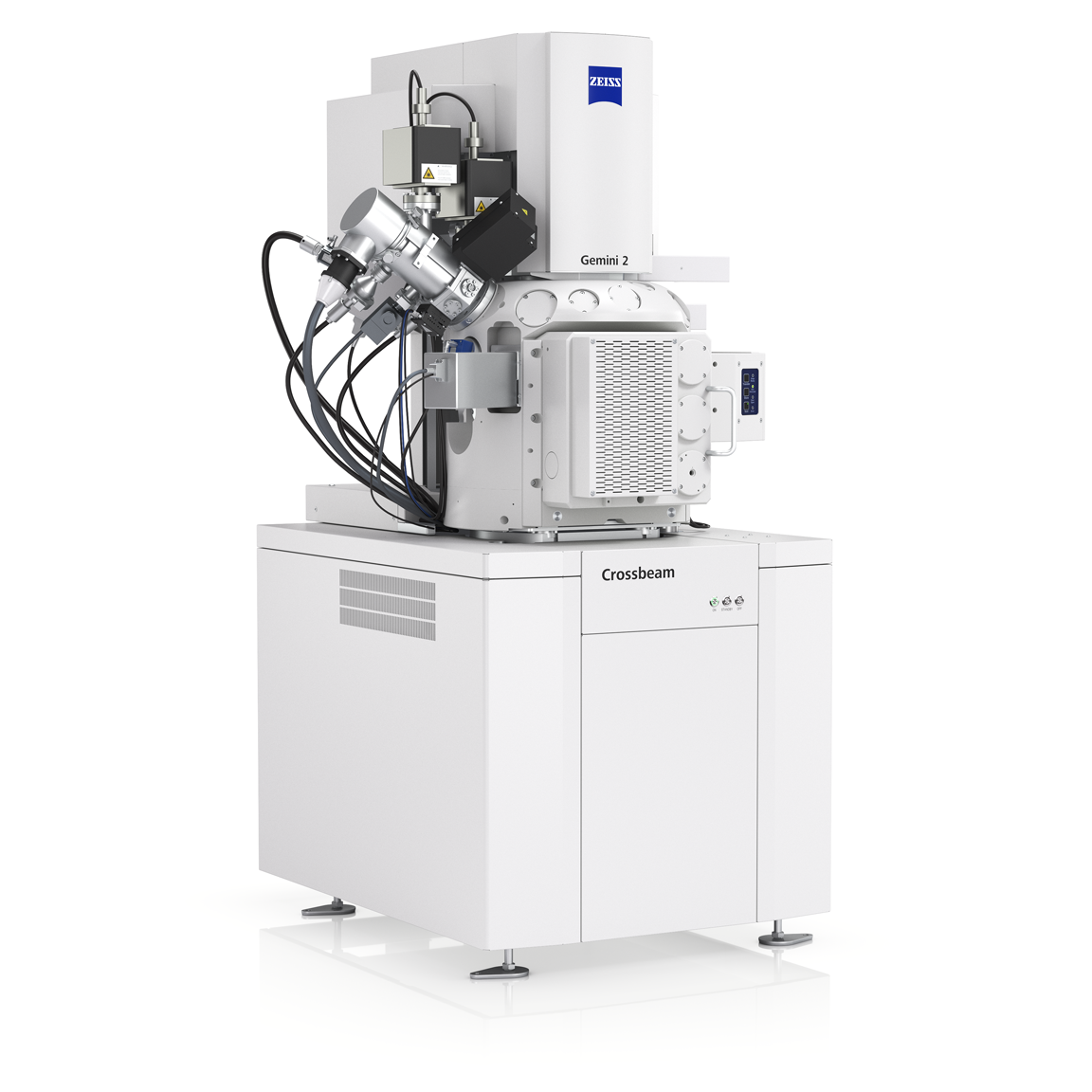
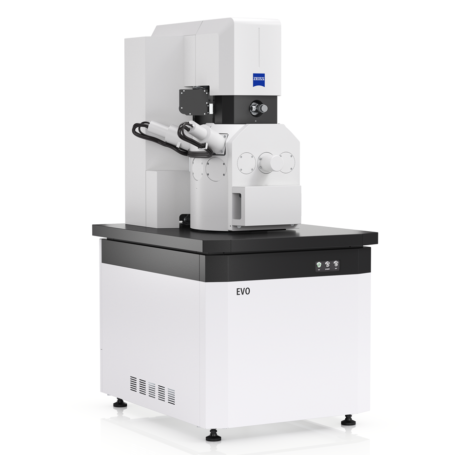
As a leading supplier of quality solutions, ZEISS offers inspiring innovations​ and services for your PCB production process. Reliable ZEISS systems are used​ by PCB manufacturers across the globe.

ZEISS Electronics solutions at every manufacturing step

Blue Line for manufactruing processes and quality requirements
  • Quality gate 1

    Incoming quality control

    Challenges​

    • Monitor surface roughness of copper foil to ensure it provides the necessary low transmission loss and high binding force​
    • Analyze surface morphology of copper foil and resin, which affects the binding force between them​

    Your benefits with ZEISS​

    • Scanning electron microscope ZEISS EVO for surface morphology analysis of copper and resin plates​
    • Confocal microscope ZEISS LSM 900 for rapid analysis of surface roughness
  • Quality gate 2

    PCB manufacturing process

    Challenges​

    • During PCB pattern manufacturing, dry film adhesion affects precision of line etching​
    • Rapid 3D size measurement of conductor and connecting hole is needed to reduce sample preparation requirements and improve detection efficiency​
    • Surface finish process affects subsequent weldability, rapid measurement of element content, and process quality control​

    Your benefits with ZEISS​

    • High-resolution metallographic section analysis using optical microscope ZEISS Axioscope​
    • Rapid check of line width and spacing with digital microscope ZEISS Smartzoom 5​
    • Confocal microscope ZEISS LSM 900 for determining size of blind hole and through hole, plus roughness​ detection​
    • Swift examination and analysis of dry film adhesion, desmear, and nickel corrosion with scanning electron microscope ZEISS EVO
  • Quality gate 3

    PCB Assembly (PCBA)

    Challenges​

    • Daily high production requires quick dimensional measurement and surface defect inspection of the welded foot
    • The quality of the solder joint will affect the integrity of the circuit, so it is necessary to find out the relevant reasons to improve the welding process

    Your benefits with ZEISS​

    • Digital microscope ZEISS Smartzoom 5 welding quality for quick inspection Optical imaging instrument ZEISS O-DETECT, welding size detection
    • Scanning electron microscopy ZEISS EVO rapid detection of IMC-layer thickness high resolution X-ray microscope ZEISS Xradia Versa

Contact us

Would you like to learn more about our solutions for industries? We are happy to provide more information or a demo.

Do you need more information?

Get in touch with us. Our experts will get back to you.

Form is loading...

/ 4
Next Step:
  • Interest Inquiry
  • Personal Details
  • Company Details

If you want to have more information on data processing at ZEISS please refer to our data privacy notice.