ZEISS Crossbeam FIB-SEM with Gemini 4 electron column for nanostructure analysis.
High-end FIB-SEM for advanced industrial analysis

ZEISS Crossbeam​

High-throughput FIB-SEM for 3D analysis

The combination of scanning electron microscope (SEM) and focused ion beam (FIB) enables precise material removal and high-resolution imaging of structures beneath the surface. ZEISS Crossbeam provides reliable solutions for failure analysis, sample preparation, and 3D material characterization – helping industrial users understand complex materials and devices with confidence.

Key capabilities:

  • Precise localization and analysis of defects
  • High-quality TEM/STEM sample preparation
  • High-resolution 3D FIB-SEM characterization
  • Flexible analytical options including EDS, EBSD, WDS, SIMS, and more
  • Extended capabilities with optional femtosecond laser integration

ZEISS Crossbeam for industry

Advanced FIB-SEM analysis for complex materials
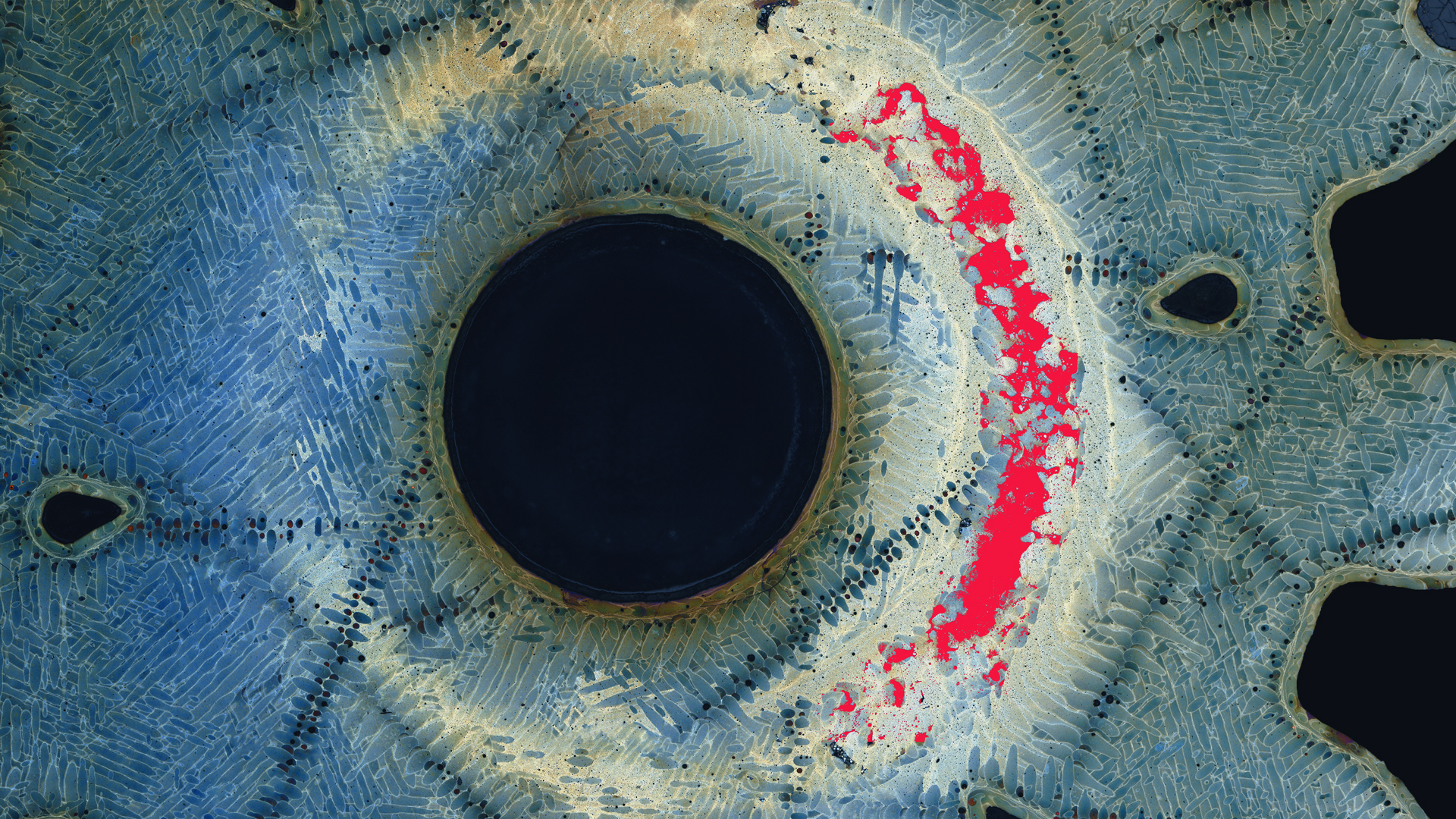
Red laser scanning a microelectronic cross-section for precision materials analysis.

ZEISS Crossbeam combines high-resolution SEM imaging and precise FIB processing for failure analysis, defect localization, TEM/STEM lamella preparation, and 3D material characterization.

Automated workflows, endpoint detection, and the Ion-sculptor FIB column enable precise, reproducible lamella preparation while minimizing sample damage.

Benefits

  • High-quality lamellae
  • Precise thickness control
  • Reproducible results

Femtosecond laser integration
Expand your capabilities with fast material removal, deeper structure access, and large-area sample preparation.
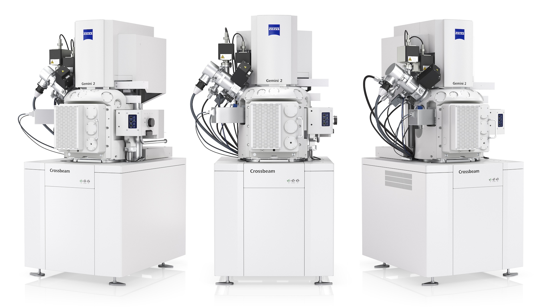
ZEISS Crossbeam FIB-SEM system configured in different ways to meet specific application requirements.

Fields of application at a glance

ZEISS Crossbeam enables precise FIB-SEM workflows for industrial material analysis, from targeted sample preparation to advanced 3D characterization.

    • Failure analysis and defect localization
    • TEM/STEM lamella preparation
    • High-resolution cross-section analysis
    • 3D FIB-SEM tomography
    • Targeted material removal and structure analysis

    New: ZEISS Crossbeam 750 for industry

    See while you mill.
    Engineer loading a sample into a ZEISS Crossbeam 750 FIB-SEM with Gemini 4 in a microscopy lab.

    ZEISS Crossbeam 750 combines high-resolution imaging, precise FIB milling, and live endpoint control in one powerful platform – enabling faster analysis, reproducible sample preparation, and reliable results for demanding industrial applications.

    Experience ZEISS Crossbeam 750

    Precision for every analysis. Confidence in every workflow.

    Discover precise, reliable FIB-SEM workflows with ZEISS Crossbeam 750 – from failure analysis and material characterization to advanced sample preparation.

    Key applications and benefits of ZEISS Crossbeam 750

    Cross-sectional SEM image showing an 858.4 μm depth measurement and 10 μm microstructural detail.

    Accelerate failure analysis

    Identify defects and root causes faster

    ZEISS Crossbeam 750 combines XRM-guided defect localization with precise FIB-SEM cross-sectioning to enable fast, reliable nanoscale failure analysis.

    Key benefits

    • XRM-to-FIB-SEM workflow
    • Targeted defect cross-sections
    • Faster root cause analysis
    • High-resolution 2D & 3D imaging
    Series of grayscale cross-sectional microscope images of layered microelectronic structures.

    Precision control for faster semiconductor analysis

    The new ZEISS solution integrates enhanced imaging, precise milling, and HDR Mill and SEM to deliver reliable process control, accurate cross-sections, and faster failure analysis for advanced semiconductor devices.

    Key benefits

    • Faster failure analysis
    • Precise nanoscale cross-sections
    • Real-time milling control
    • Improved process reliability
    • Reliable sample preparation

    Precision TEM sample preparation

    High-quality lamellae with real-time control

    ZEISS Crossbeam 750 enables precise TEM and STEM lamella preparation with live endpoint control. Continuous process monitoring ensures accurate milling, optimal lamella thickness, and reduced sample damage.

    Key benefits

    • Precise targeting of regions of interest
    • Reduced risk of over-milling and rework
    • Reproducible lamella quality

    Reveal hidden 3D structures

    High-resolution 3D insights beyond the surface

    Automated FIB-SEM tomography with precise endpoint control enables accurate 3D reconstruction and analysis of microstructures, interfaces, and defects.

    Key benefits

    • Automated slice & view workflows
    • Precise endpoint control
    • High-resolution 3D characterization
    ZEISS Crossbeam 750 FIB-SEM in a microscopy lab with analysis software on screen.

    Increase productivity with intelligent automation

    Standardize workflows and improve efficiency

    The new system enables automated FIB-SEM workflows that reduce manual intervention, improve reproducibility, and deliver consistent results across operators and samples.

    Key benefits

    • Automated FIB-SEM workflows
    • Reduced manual effort
    • Consistent and reproducible results
    • Higher efficiency for demanding industrial analysis
    ZEISS Crossbeam 750 FIB-SEM with workstation for materials analysis and sample preparation.

    ZEISS Crossbeam 750 for advanced industrial applications

    Advanced process control, automation, and reproducibility ensure reliable results in demanding workflows.

    Applications

    • Semiconductors & electronics
    • Batteries & advanced materials
    • Additive manufacturing
    • Quality & process optimization

    Learn more in our videos about ZEISS Crossbeam
    • Fast 3D failure analysis.correlative workflow solution from ZEISS.​

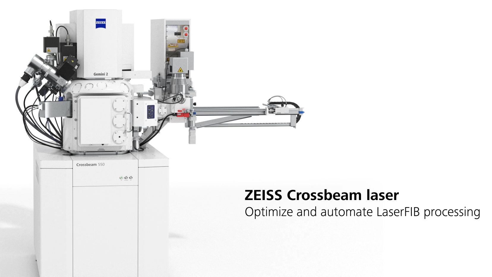
    • ZEISS Crossbeam Laser: Optimize and automate processes with LaserFIB​

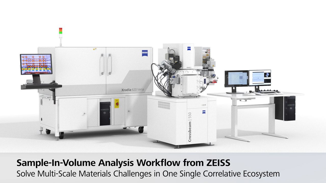
    • Learn more about the sample-in-volume analysis workflow.​

    • ZEISS Crossbeam 750 FIB-SEM with workstation for materials analysis and sample preparation.

      Experience ZEISS Crossbeam 750

    • Watch the video about our correlative workflow solution! Learn how easy it is to use your data across technologies with ZEISS Solutions and how to achieve reliable and efficient results.​
      Fast 3D failure analysis.correlative workflow solution from ZEISS
    • 1. Gain rapid access to deeply buried structures 2. Perform laser work in a dedicated integrated chamber to maintain cleanliness of your FIB-SEM main chamber and detectors 3. Automate laser processing, polishing, cleaning and transfer of the sample to the FIB chamber 4. Prepare multiple samples e.g. cross-sections,TEM lamellae, pillar arrays. Work efficiently by using pre-installed recipes for different materials​
      ZEISS Crossbeam Laser: Optimize and automate processes with LaserFIB​
    • Explore the sample-in-volume analysis workflow, a new instrument able to solve multi-scale materil challenges in one single correlative ecosystem. Using a range of microscopy techniques this workflow enables the user to understand the material properties linked to each scale.​
      Learn more about the sample-in-volume analysis workflow
    • Experience ZEISS Crossbeam 750

    FIB-SEM failure analysis on car body parts​

    • Engineer inspecting a car body surface for quality control in automotive manufacturing.

      Due to greater manufacturing quality and cutting-edge surface finishing technologies, defects are now smaller and less frequent. Microscopic methods must therefore be used to find, locate, prepare, and investigate surface defects and their root causes. This brochure outlines a correlative microscopy approach for efficient investigation during failure analysis.​

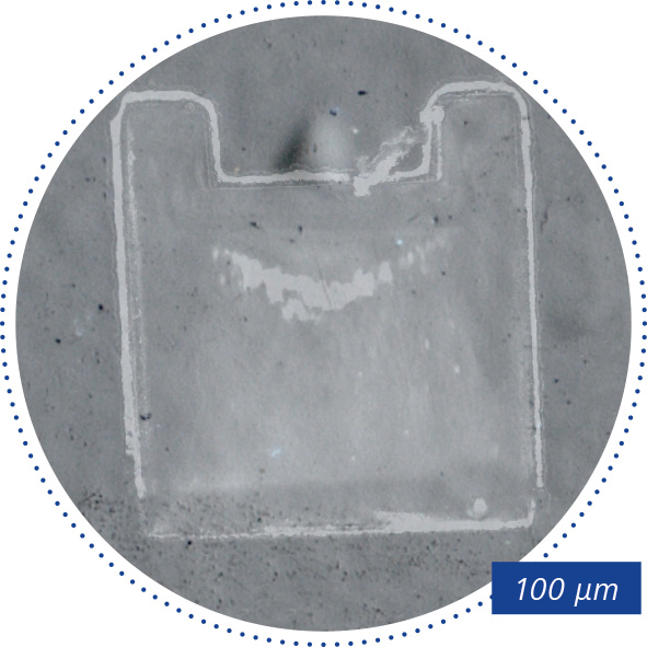
    • Cross-sectional microscope image of a milled cavity structure with 100 µm scale.

      01 Overlay of laser-milled trench on light microscope image of ROI.​

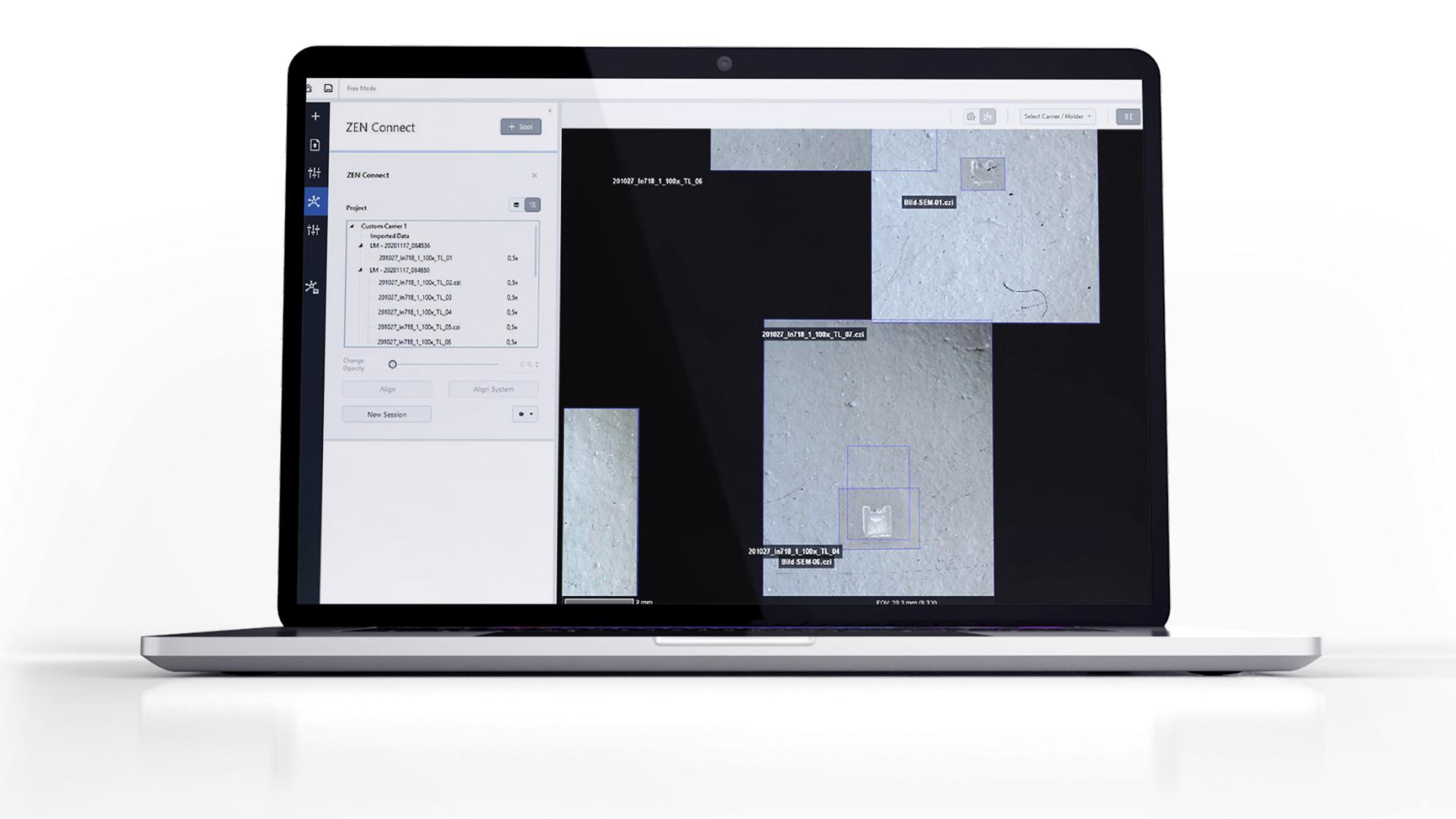
      In this context, light microscopy tasks are handled by the ZEISS Smartzoom 5 digital microscope, preparation and investigation are carried out with the ZEISS Crossbeam laser, and both systems are correlated by ZEISS ZEN Connect for precise defect relocation in the FIB-SEM.​

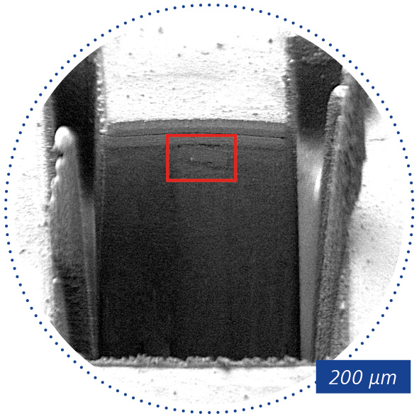
    • Cross-sectional microscope image highlighting a small defect area in red, with 200 µm scale.

      02 Laser-milled cross section through surface defect, suspicious feature visible beneath paint layers; SEM, SESI, 50x.​

      Finding the root cause of sparsely distributed and small defects on large samples for efficient failure analysis requires a convenient workflow of locating, documenting, re-locating, preparing, and investigating regions of interest. ​

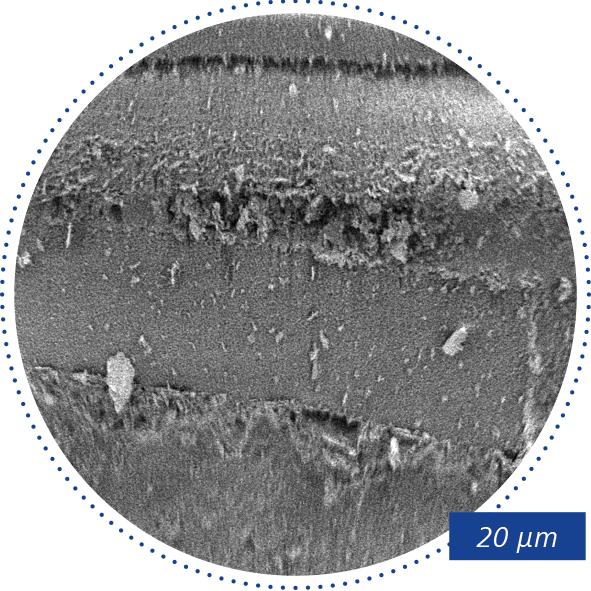
    • High-magnification cross-sectional microscope image of a rough material interface with 20 µm scale.

      03 Suspicious feature in base material underneath paint, laser-milled surface; SEM, SESI, 450x.​

      Scanning electron microscopes with a focused ion beam (FIB-SEM) overcome the limitations of conventional materialographic sample preparation. However, since electron microscopes typically have a limited field of view, it is sometimes easier to perform the localization step on a light microscope. For this reason, users need a system that allows them to localize the image area in the light microscope and then retrieve it in the FIB-SEM.

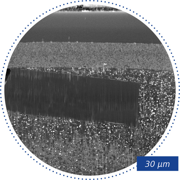
    • Grayscale cross-sectional microscope image of a layered material sample with 30 µm scale.

      04 FIB post-polishing, good surface finish with clearly distinguishable features; SEM, InLens, 450x.​

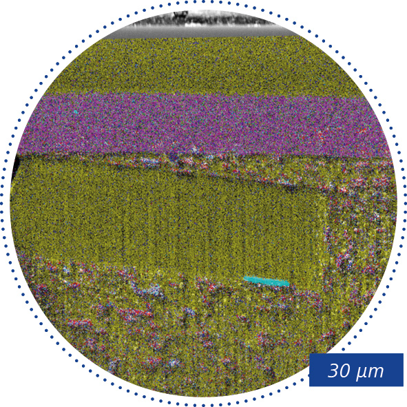
      The ZEISS ZEN Connect software solution combines with ZEISS ZEN Data Storage to provide exactly this. The new femtosecond laser for the ZEISS Crossbeam family also offers location-specific preparation in large areas. With the help of fs-laser and FIB cross-section polishing and EDS analysis, the cause of the surface defects in the above example was determined as carbon fiber scraps. ​

    • Color-coded cross-sectional microscopy image of a layered material structure with 30 µm scale.

      05 EDS element mapping of FIB-polished area; yellow: C intensity, blue: Al intensity, pink: Ti intensity, red: Si intensity.​

      The correlative microscopy approach also enables efficient investigation of more than one area of interest. All results are subsequently saved in a coherent project, with the ZEISS ZEN Data Storage option ensuring full accessibility for further investigation or reporting.​

    Laptop showing ZEISS ZEN Connect software with stitched microscopy images and sample navigation view.

    Overlay of laser-milled trench on light microscope image of ROI; SEM, SESI, 450x. ​

    Download information

    • ZEISS Crossbeam 750 550 350 product info PDF EN

      26 MB
    • ZEISS Crossbeam750 flyer semiconductor PDF EN pdf

      4 MB
    • ZEISS Flyer Crossbeam750 Materials EN PDF

      661 KB
    • ZEISS IMS SEM Brochure Portfolio EN PDF

      22 MB
    • ZEISS IQS Technical Paper, FIB/SEM, Failure analysis, EN, PDF

      5 MB
    • Battery Material High Resolution 3D Imaging by FIB

      6 MB


    Contact us​

    Interested in exploring our products or services further? We're excited to offer you more details or a live demo, either remotely or in person.​

    Do you need more information?

    Get in touch with us. Our experts will get back to you.

    Form is loading...

    / 4
    Next Step:
    • Interest Inquiry
    • Personal Details
    • Company Details

    If you want to have more information on data processing at ZEISS please refer to our data privacy notice.