Shaping the future of microchip manufacturing
Erik Loopstra and Vadim Banine named European Inventor Award 2018 finalistsMunich/Oberkochen, Germany | 24 April 2018 | ZEISS Semiconductor Manufacturing Technology
Erik Loopstra and Vadim Banine have been nominated for their inventions in the field of Extreme Ultraviolet Lithographie (EUV). Erik Loopstra, originally from ASML, has been working since years at ZEISS business group Semiconductor Manufacturing Technology closely with ASML and ZEISS employees. Vadim Banine is Director of Research of ASML.
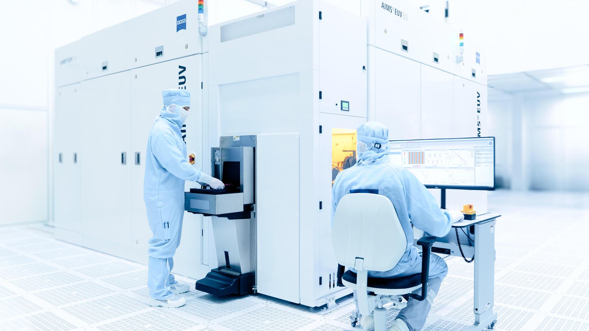
Erik Loopstra and Vadim Banine have been nominated by the European Patent Office (EPO) as finalists for the European Inventor Award 2018 in the category "Industry". The key invention of systems engineer Erik Loopstra, physicist Vadim Banine and their research and engineering teams in the field of extreme ultraviolet lithography (EUV) have made it possible to create geometric patterns on silicon wafers – the basis of the microchip – at a previously unprecedented level of detail. The resulting process not only upholds Moore’s Law, but also makes it possible in the future to create chips with details as small as 8 nanometres.


After two decades of development in close cooperation with research partners and suppliers, ASML and its strategic partner Carl Zeiss SMT GmbH brought EUV to market in a complete product in 2017. Now it is possible to produce chips, marking a generational shift over older methods, which are more time-consuming than EUV Lithography and require several passes through the lithographic printing. The technology promises to save chipmakers time and money in the production of the next generations of chips that will drive innovations in fields such as consumer electronics, health, entertainment, autonomous driving, robotics and artificial intelligence.
“With constantly increasing functionality, modern computer chips have to process ever larger amounts of data at an ever faster pace. At the same time, neither energy consumption nor production costs per chip should increase. This development can only be continued if the number of integrated circuits found on a microchip rises constantly. This is exactly, what EUV allows,” said Dr. Karl Lamprecht, Member of the Executive Board of the ZEISS Group and President and CEO of Carl Zeiss SMT GmbH. EPO President Benoît Battistelli adds: "By combining their respective skills as a physicist and systems engineer, Banine and Loopstra have significantly contributed to develop a technology for industrial use that will help manufacture the next generations of microchips.”
The winners of this year's edition of the EPO's annual innovation prize will be announced at a ceremony in Paris, Saint-Germain-en-Laye, on 7 June 2018.
The European Inventor Award is one of Europe's most prestigious innovation prizes. Launched by the European Patent Office in 2006, it honors individual inventors and teams of inventors whose pioneering inventions provide answers to some of the biggest challenges of our times.