
Building the future with stronger, tougher, lighter and sustainable metals and alloys
Metals and alloys is a key research topic around most academic materials science programs. Imagine being able to engineer microstructure and thus enhance mechanical, thermal and electrical properties. You will be able to use precise control of the grain size, engineer grain boundaries and precipitates, control the presence of defects such as inclusions or voids. You will achieve remarkable improvements in the properties of traditional metals and alloys and thus create more useful materials.

Macroscale Features
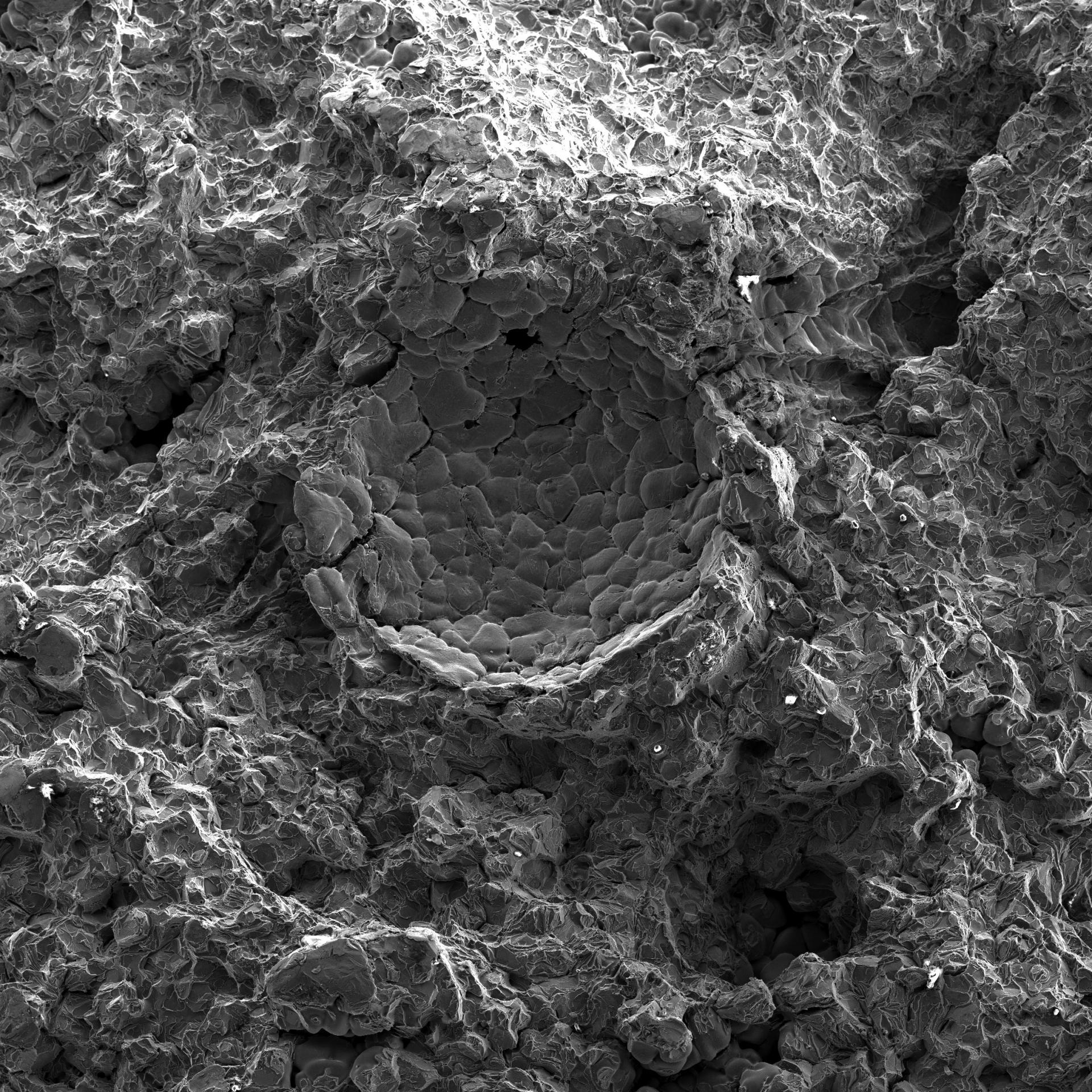
Understanding the interdependencies of macro-, micro- and nanostructureEffectively characterize material at the macroscale and gain insights related to geometric defects, surface roughness, cracks, voids and inclusions. Use a combination of ZEISS light and X-ray microscopes (XRM).


.")
.")


.")
.")
.")
.")


From Micro- to Nanoscale
Comprehensive characterization with a scanning electron microscopeThink of the possibilities it would open if you found a solution to characterize materials from micro- to nanometer with one instrument. You would be able to set up a workflow for root cause analysis enabling you to study the relationship between microstructure and fracture resistance or understand structural failures of critical parts. You could determine fracture modes and analyze crack propagation. What if you could analyze the chemical composition of precipitates and inclusions in detail over multiple length scales; describe grain characteristics including size, crystal orientation, shape, boundaries, and phase distribution; understand deformation behavior of metals and alloys? And, finally, modify the materials processing route and chemistries and fine tune their properties and performance? In fact, scanning electron microscopes (SEM) and their accessories have become an integral part of the materials characterization workflow. To many researchers the SEM is the go-to instrument, the “Swiss-knife“.
Assess Grain Characteristics and Deformation Behavior
-
- Energy dispersive X-ray spectroscopes (EDS) enable you to understand chemical makeup and elemental distributions.
- Measure grain size and shape, crystallographic orientation, texture, and grain boundary character distribution over scales from a few micrometers down to 10 nm using electron backscattered diffraction (EBSD).
- Use electron channeling along crystal planes and apply electron channeling contrast imaging (ECCI) letting you observe and quantify lattice defects directly.
- Identify dislocations and stacking faults within grains and describe their location with respect to grain boundaries and orientations.
- Combine ECCI with in situ deformation or heating experiments of metal samples to observe the formation of dislocation networks under the influence of mechanical loads.


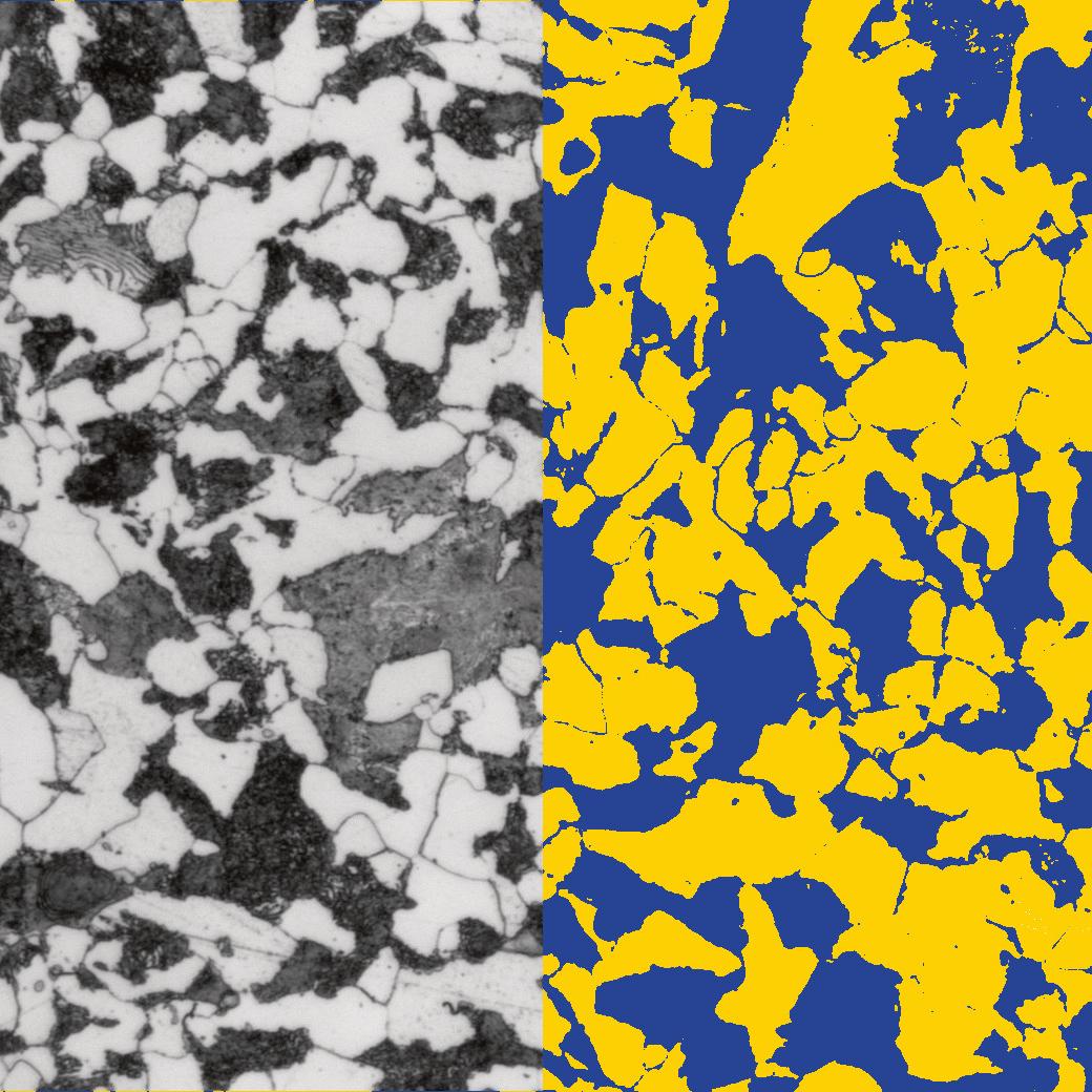
EDS mapping of a conspicuous mixed inclusion. The core of the mixed inclusion consists of the "typical" inclusion types MnS (red) and Al2O3 (blue) whereas the surrounding bright phase contains the elements Bi (yellow) and P (green).
EDS mapping of a conspicuous mixed inclusion. The core of the mixed inclusion consists of the "typical" inclusion types MnS (red) and Al2O3 (blue) whereas the surrounding bright phase contains the elements Bi (yellow) and P (green).


 delivers extremely high contrasts of crystal orientations and defects in the high temperature alloy TiAl₂.")
 delivers extremely high contrasts of crystal orientations and defects in the high temperature alloy TiAl₂.")


 delivers extremely high contrasts of crystal orientations and defects in the high temperature alloy TiAl₂.")
 delivers extremely high contrasts of crystal orientations and defects in the high temperature alloy TiAl₂.")
 delivers extremely high contrasts of crystal orientations and defects in the high temperature alloy TiAl₂.")
 delivers extremely high contrasts of crystal orientations and defects in the high temperature alloy TiAl₂.")


Broaden opportunities at the Mesoscale
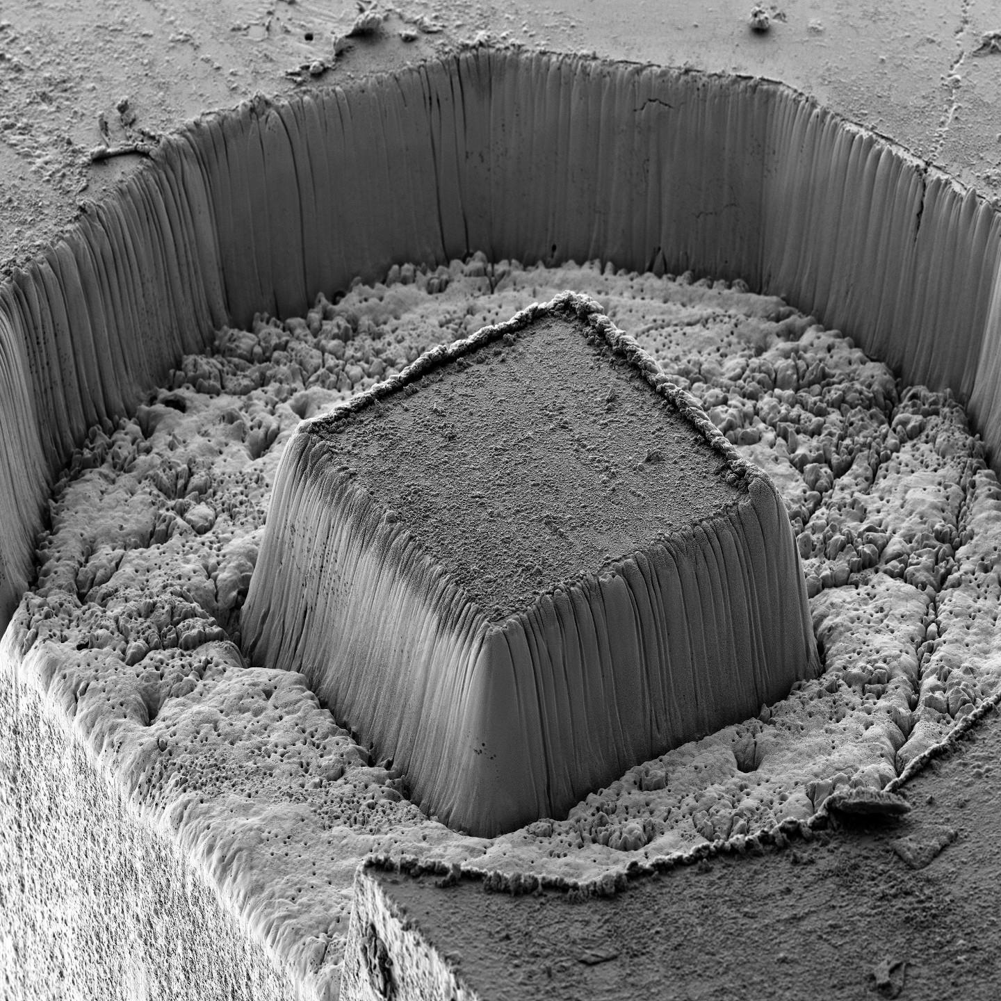
Machine nano-, micro- or meso-scale structures and enhance high-resolution sub-surface microstructural characterizationInvestigating metals and alloys down to the level of individual atomic arrangements while keeping the full context over a scale of millimeters is critical. Only the combination of both, overview over millimeter- and detailed insight into micro- or nanometer-scaled areas, enables you to understand the linkage between structure and properties.


. The cube has side walls of 180 µm length and is 120 µm tall. Laser machining time 85 s. FOV 696 µm. ZEISS Crossbeam 350 laser, SESI detector, 5 kV.")
. The cube has side walls of 180 µm length and is 120 µm tall. Laser machining time 85 s. FOV 696 µm. ZEISS Crossbeam 350 laser, SESI detector, 5 kV.")


. The cube has side walls of 180 µm length and is 120 µm tall. Laser machining time 85 s. FOV 696 µm. ZEISS Crossbeam 350 laser, SESI detector, 5 kV.")
. The cube has side walls of 180 µm length and is 120 µm tall. Laser machining time 85 s. FOV 696 µm. ZEISS Crossbeam 350 laser, SESI detector, 5 kV.")