webinar

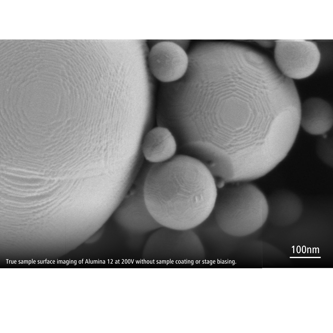
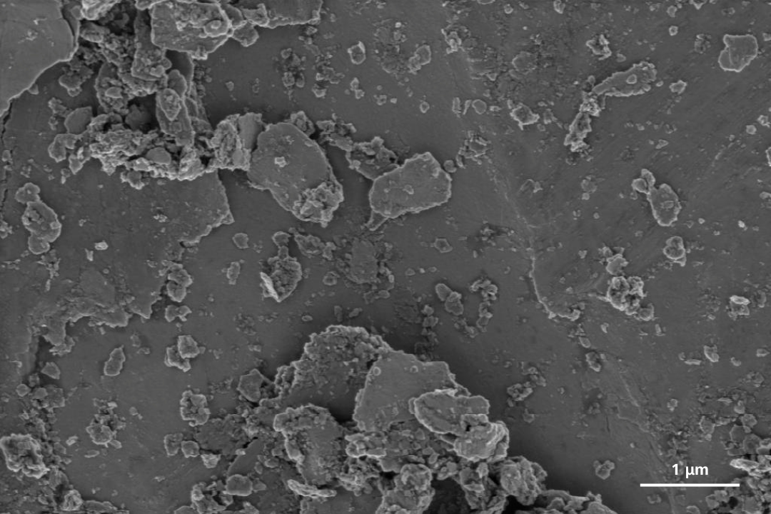
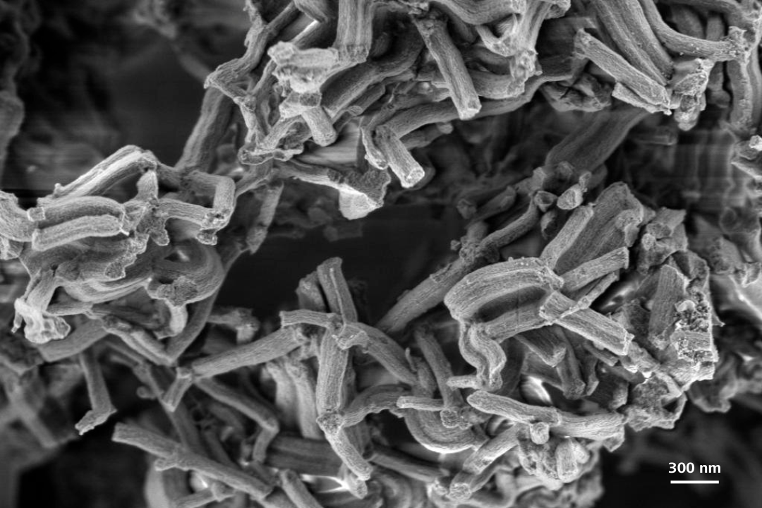
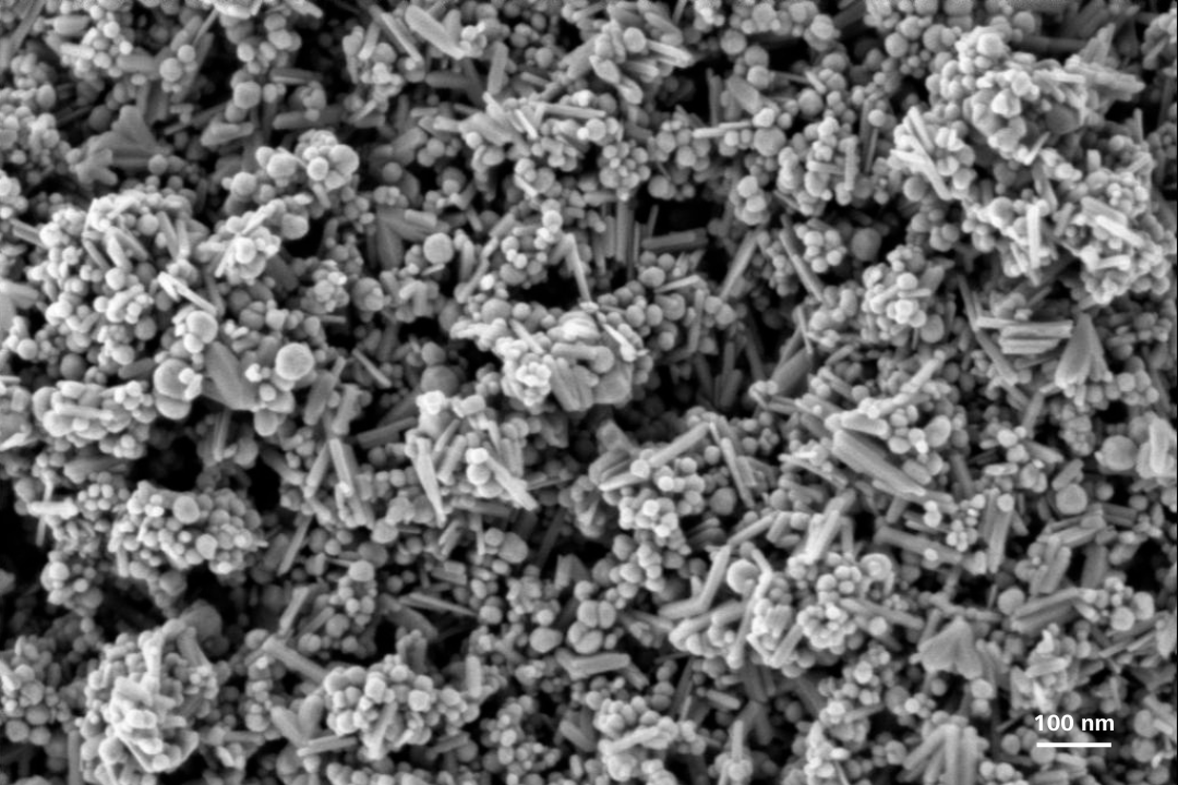
Achieve true sample surface imaging with low & ultra-low kV

With the ZEISS Gemini 3 column

High resolution SEM imaging of non-conductive & magnetic surfaces without surface coating is desirable as it enables the investigation of unobstructed topographical information of a sample.

In order to achieve high resolution true sample surface imaging, the use of low accelerating voltage is preferred, however low or ultra-low kV SEM imaging present its challenges which include:
(i) Poor signal-to-noise ratio
(ii) Low image resolution
(iii) Image distortion due to poor alignment of low energy beam

Learn how the combination of the new Nano-twin lens and Smart Autopilot (a new electron optical engine) on the ZEISS Gemini 3 column has worked synergistically to enable sub-nanometer resolution imaging on non-conductive and magnetic surfaces at low and ultra-low kV.

Click register below to attend the free webinar & learn how to...

  1. Perform high resolution imaging at ultra-low kV without surface coating or stage biasing for true sample surface imaging
  2. Maximize compositional contrast even at low kV
  3. Perform sweet spot imaging with flexible imaging parameters
  4. Perform distortion-free magnetic nanoparticles imaging
  • High resolution imaging of Mesoporous silica nanomaterials at 500V without sample coating or stage biasing.

    High resolution imaging of Mesoporous silica nanomaterials at 500V without sample coating or stage biasing.

1. High resolution imaging at ultra-low kV for true sample surface imaging

Learn how the beam booster technology, Smart Autopilot and Nano-twin lens on the Gemini 3 column worked synergistically to reduce the spread of the primary beam, minimize the effect of lens aberration and ensure excellent signal detection efficiency to support high resolution imaging at ultra-low kV.

Witness the Ultra-low kV imaging effect on non-conductive samples such as mesoporous silica, SiC fibers & CNTs where high resolution images on highly magnified samples were used. These samples were imaged between 0.5 to 1 kV without surface coating or stage biasing.

  • Tungsten Nickel Iron Alloy: EsB detector for BSE image with compositional contrast.

  • Tungsten Nickel Iron Alloy: Inlens detector for SE image for surface topography.

    Tungsten Nickel Iron Alloy: Inlens detector for SE image for surface topography.

2. Maximize compositional contrast at low kV

Learn how the electrostatic lens and in-column Energy Selective Backscatter (EsB) filter grid on the Gemini 3 column facilitate the trajectory of electrons back into the column for enhanced in-column signal detection.

The use of filter grid ensures excellent selection of backscattered electrons signal for enhanced compositional contrast imaging at low kV.

The samples featured in this section include NiO doped CNT, tungsten alloy and silicon dioxide alumina doped nanoparticles.

Witness the distinct compositional contrast between Inlens detection used for topography imaging and EsB detection for compositional contrast imaging.
 

  • Zeolites with 1.0 mm working distance for superior unobstructed surface topography imaging.

    Zeolites with 1.0 mm working distance for superior unobstructed surface topography imaging.

3. “Sweet spot" imaging with flexible imaging parameters

Gain free control of imaging parameters e.g., working distance to obtain the best topographical contrast during low kV imaging.

The Gemini 3 column does not require stage biasing at low kV imaging hence no restriction to the working distance.

Learn how enhanced topographical contrast can be achieved by reducing accelerating voltage and working distances for samples such as CNT, Silicon Dioxide microparticles and carbonaceous thin film material.

  • Magnetite nanomaterials imaged at 1kV and WD of 0.9mm.
     

    Magnetite nanomaterials imaged at 1kV and WD of 0.9mm.
     

4. Distortion-free magnetic nanoparticles imaging

Discover how the nano-twin lens on Gemini 3 column with well overlap electrostatic and magnetic field distributions significantly reduce residual magnetic field on the sample surface. Together with the Inlens detector that is designed for efficient detection of secondary electrons at low kV imaging, these characteristics support sub-nanometer imaging below 1kV for magnetic samples.

The high resolution imaging of the Magnetite sample was imaged at working distance as low as 0.9 mm, indicating very low magnetic field experienced on the sample.

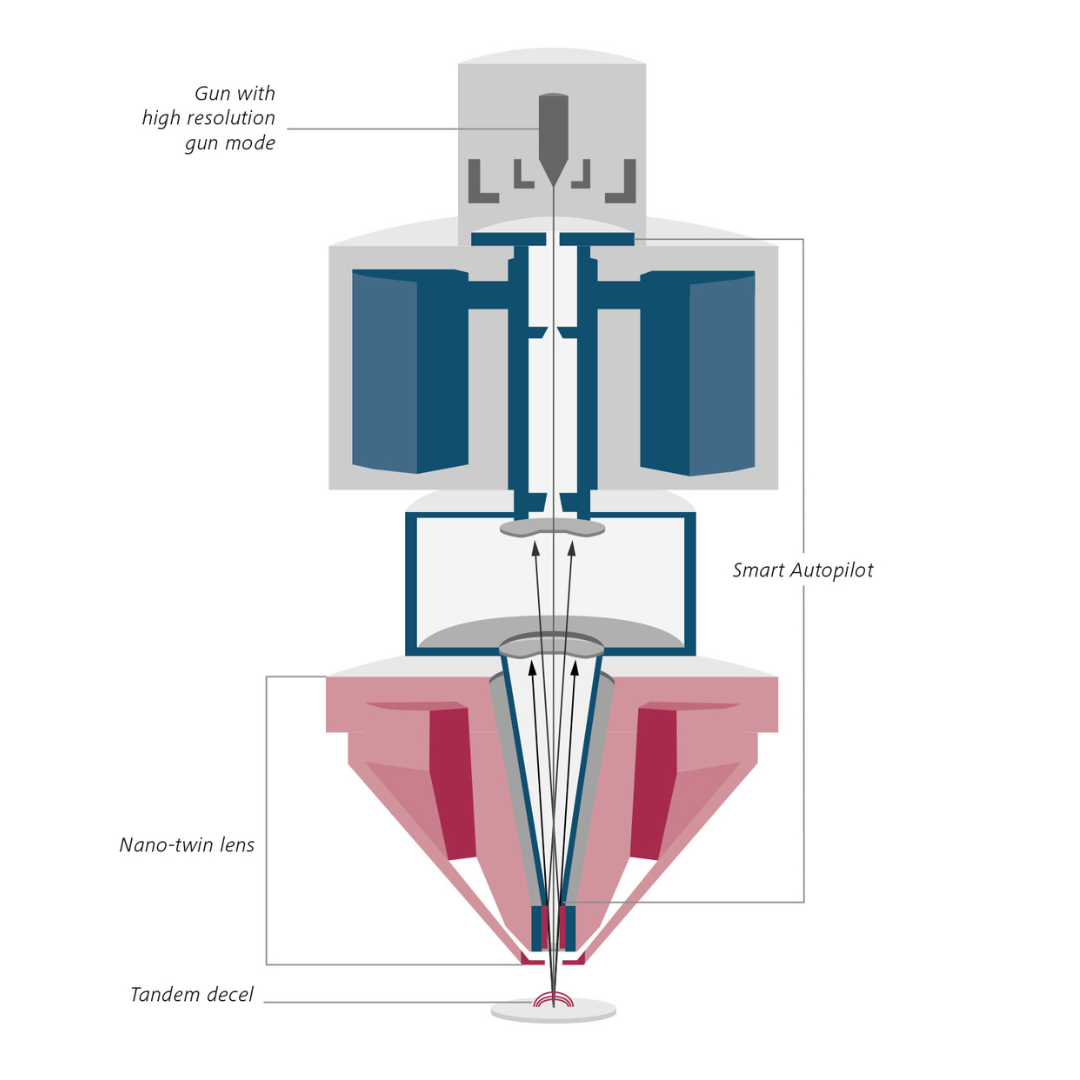
Introducing the Gemini 3 Column

Gemini 3 optics are optimized for resolutions at low voltages and for contrast enhancement. Sub-nanometer imaging below 1 kV is now possible without immersing the sample in an electro-magnetic field. Maximum resolution at all working conditions from 1 kV to 30 kV is ensured.

Gemini 3 consists of two components which work synergistically: the Nano-twin lens and Smart Autopilot, a new electron optical engine.

The Nano-twin lens delivers sub-nanometer resolution at low voltages with excellent signal detection efficiency. It works with significantly reduced lens aberrations at low kV compared to the standard Gemini objective lens and the Inlens detector signal is enhanced under low voltage imaging conditions.

In combination with the Nano-twin lens, Smart Autopilot lets you benefit from the best possible resolution at each working condition through condenser optimization of the beam convergence angle.

Switch seamlessly between sample navigation and high-resolution imaging with a large field of view overview mode. Achieve optimum image quality at high speed with a new autofocus.

Register for the free low kV imaging webinar

Fill out the form to reserve your place

Form is loading...