
Controlled Electron Channeling Contrast Imaging
A New Perspective for Defect Analysis in Bulk Samples without a TEM● Introduction to ZEISS Gemini column electron microscopy
● How to observe extended crystal lattice defects like dislocations and stacking faults.
● The basic principle of contrast formation, and how electrons channel into a crystal lattice when the incident beam hits the lattice along the Bragg angle.
● What is required for a methodical workflow involving a suitable scanning electron microscope with optimal beam conditions coupled with a sophisticated crystallographic analysis software.

About the Webinar
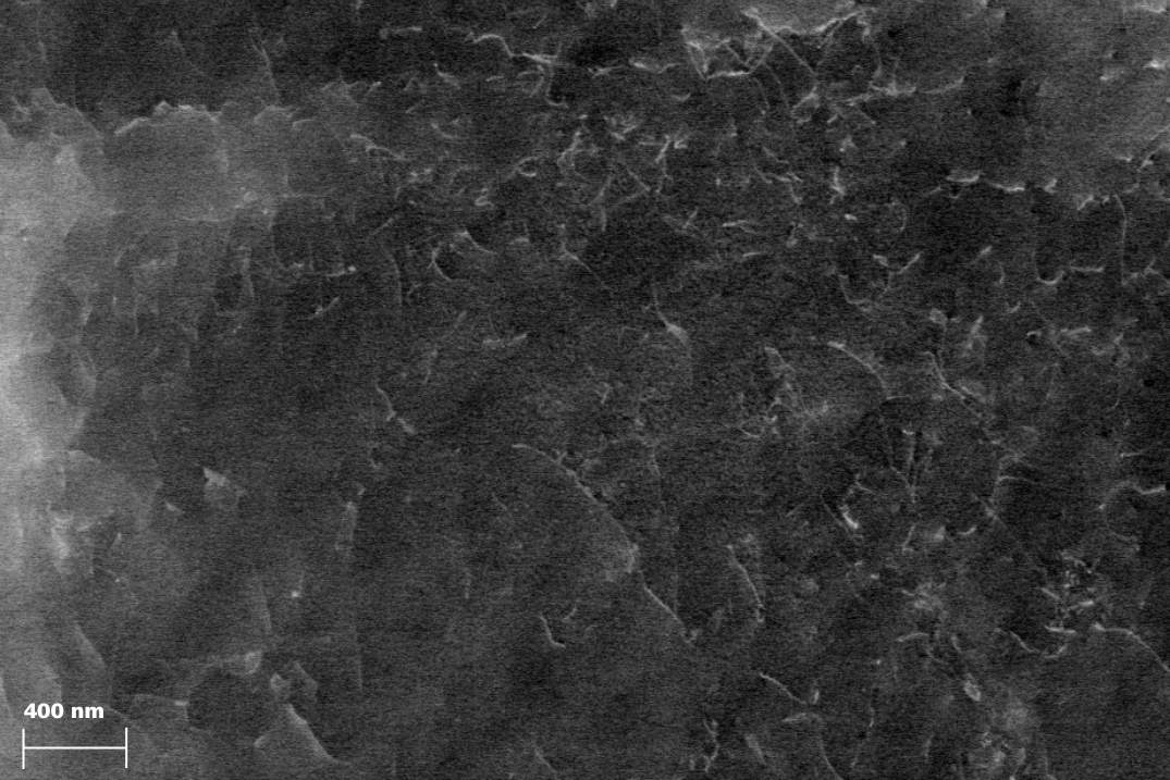
Discover a new approach to characterize dislocations in bulk samples with a scanning electron microscope (SEM) in this webinar. We invite you to explore how to visualize crystallographic defects in polycrystalline materials using controlled electron channeling contrast imaging (cECCI) in an SEM.
Join us as we highlight the potential of cECCI and how it enables the observation of extended crystal lattice defects such as dislocations and stacking faults. It exploits the dependence of backscattered electron intensity on crystal orientation and atomic order.
We will explain the basic principles of electron channeling contrast, the importance of determining the perfect imaging condition, and how any defect that disturbs the order of the lattice planes is made visible. Learn how to navigate the challenges of ECCI's low contrast intensity and master the necessary controlled workflow for optimal results.
The method requires a SEM with optimal beam conditions and sophisticated crystallographic analysis software. The advantages over TEM (transmission EM) are that you are no longer limited to thin films as you can now observe bulk samples. This allows you to benefit from simplified sample preparation, facilitated in-situ experiments, and access to true sample representivity.
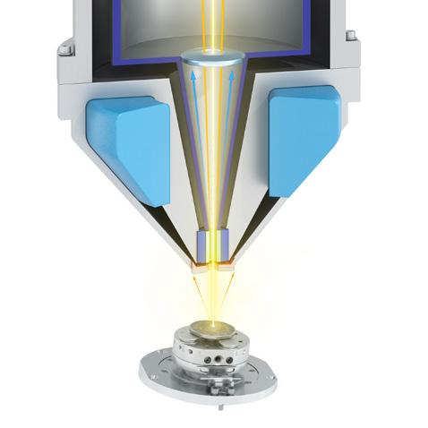
Don't miss this opportunity to enhance your understanding of the basic principles of cECCI utilizing a ZEISS field emission SEM (FE-SEM) with Gemini electron optics and TOCA (Tools for Orientation Determination and Crystallographic Analysis) software, exemplified with application examples ranging from metals and intermetallics to semiconductors and insulators such as ceramics and geological materials.
Webinar Speakers


Born in Germany's largest coal and steel area, the Ruhr-Area, he developed already as a young boy a strong interest in microscopy and the “smallest things”. He studied materials science and electron microscopy at the TU Clausthal, Germany, and obtained his PhD on a TEM investigation on textures and microstructures in titanium alloy. After post doc times in Paris (almost 3 years) and Kyoto (almost 2 years), he joined the Max-Planck-Institute for Iron Research and became leader of the group “microscopy and diffraction” in the department of microstructure physics headed by Prof. Dierk Raabe. Since 2010 he is also lecturer at the RWTH Aachen. His main research interests are the development of new tools for electron diffraction techniques, in particular in scanning electron microscopy, and their application to understand mechanisms of microstructure and texture formation in metals, alloys, but also in geomaterials. He has authored or co-authored about 150 journal papers and a few books. His most recent work is the third edition of “Introduction to Analysis” by Engler, Zaefferer and Randle.


Hrishikesh Bale is the Market Sector Manager for Engineering Materials at ZEISS RMS. He specializes in applications development for laboratory 3D X-ray imaging techniques. His research focus lies in 3D diffraction contrast tomography and in situ micro- and nano-mechanical testing using X-ray computed tomography. He has a strong background in materials science and mechanical engineering, with over a decade of experience in synchrotron X-ray microscopy and tomography.