

Efficient solutions for your challenges.
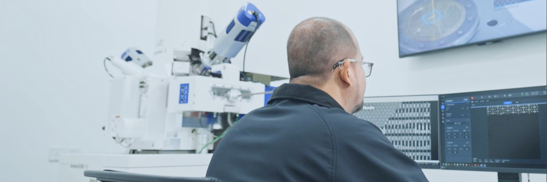
In semiconductor failure analysis, you encounter common obstacles—complex setups, time-consuming recalibrations, and tools that slow you down. It's time to streamline your workflow.
Skip to main content
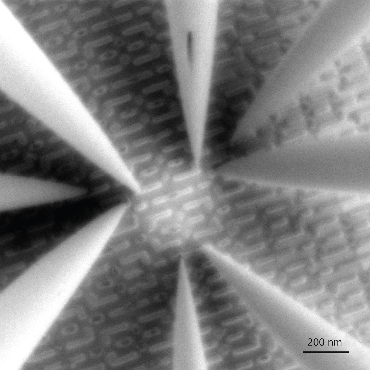
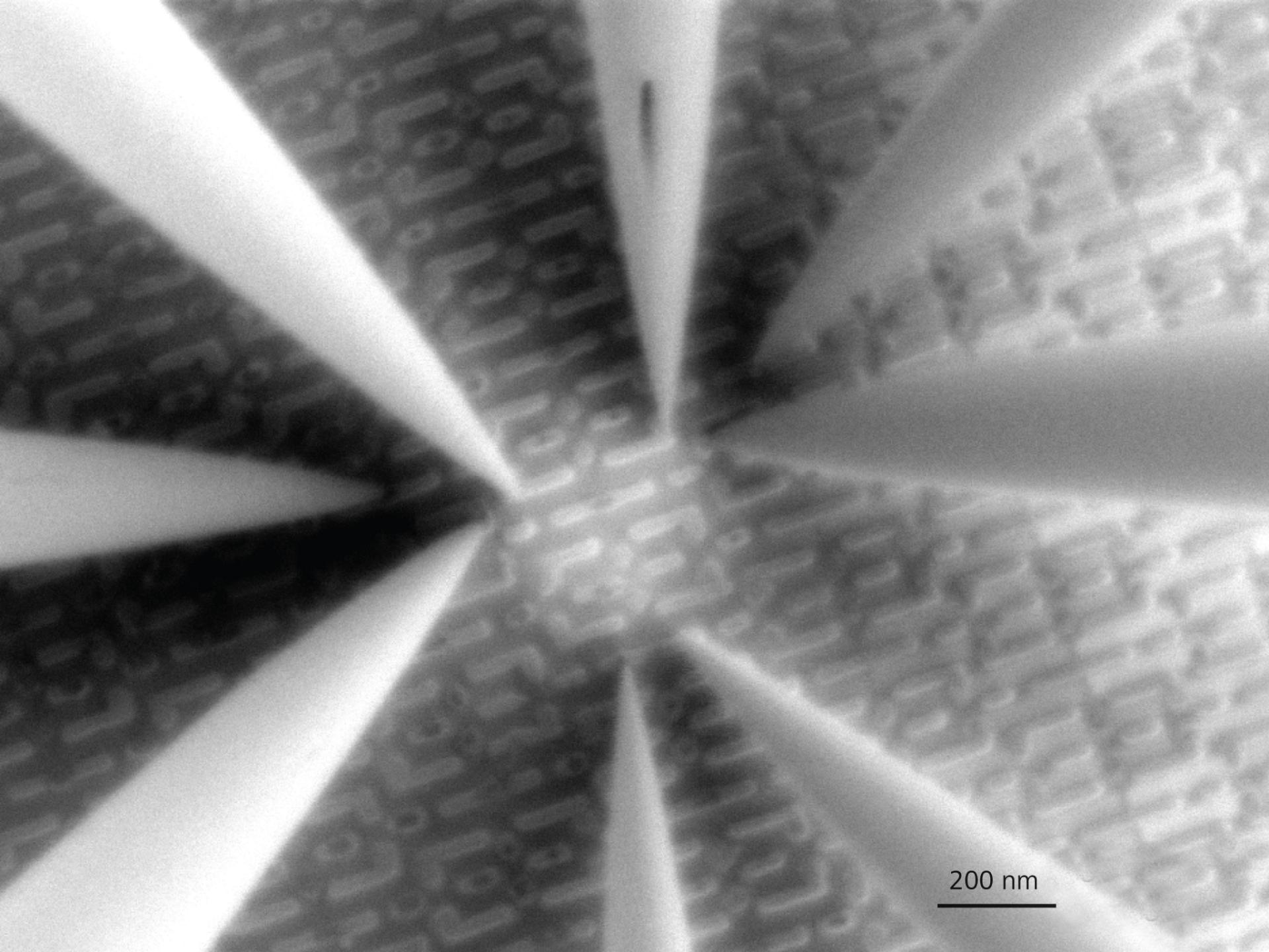
Advanced semiconductor devices demand precise imaging to identify defects. But conventional detectors make it hard to see every detail when it matters most.
ZEISS advanced detectors, including the Rapid BSD and ESB detector, deliver superior imaging capabilities. The Rapid BSD enhances high-kV imaging with subsurface sensitivity, while the ESB detector provides high-contrast imaging for materials analysis and topography. Reduced noise and enhanced clarity allow for better insight into your analysis.
Switching between beam energies should not disrupt your workflow. Yet, many systems require refocusing, stigmation adjustments, and realignment each time you change the beam, which wastes valuable time.
With our precise system calibration and stable column, beam transitions happen smoothly without sacrificing focus or field of view. This minimizes downtime and keeps your work progressing efficiently.
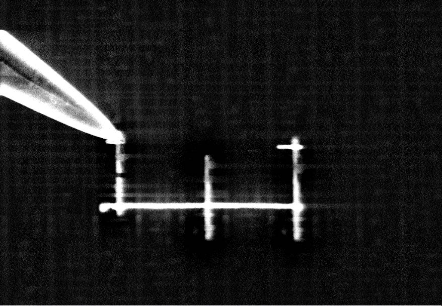
Light microscopy (LM) is your reference tool along multiple steps in the FA workflow. LM can give you insights into defects that electron microscopes (EM) cannot see, and vice versa. For navigation, communication and reporting, it is helpful to be able to correlate between LM and EM images.
ZEISS’ correlated microscopy lets you jump from LM to EM in just a few clicks. No manual matching, no wasted time. You get to the exact area you need faster, so you can diagnose issues and close out jobs with precision and speed.