Explore the Variety of Possibilities for Nanomaterials
Discover Various Applications Summarized in a 65-page eBook
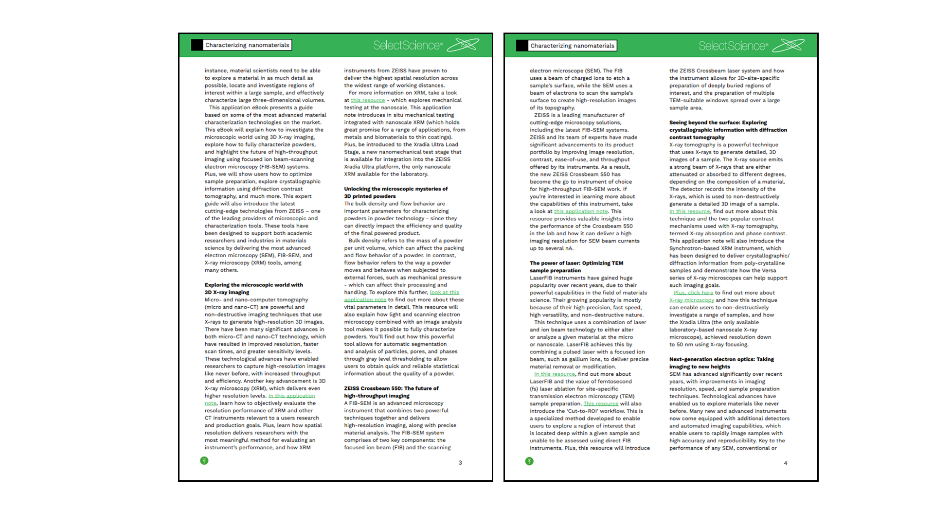
Discover a variety of applications summarized in an ebook, presenting some of the most advanced material characterization technologies on the market. Furthermore, the guide also highlights the future of high-throughput imaging using focused ion beam-scanning electron microscopy (FIB-SEM) systems.
Characterizing Nanomaterials with Precision
Explore the Latest Cutting-Edge Technologies for Nanomaterials
As the demand for faster, smaller, and more cost-effective electronics remains high, so does the need for researchers to innovate and develop novel solutions that deliver superior performance, speed, and reliability. In this context, the ability to create new material utilizing nanomaterials becomes more important. These innovations are driving the development of new and exciting technologies, and part of this change is the ability for users to characterize materials with more precision than ever before.
Discover what challenges and applications fellow researchers address using microscopy summarized in an eBook.
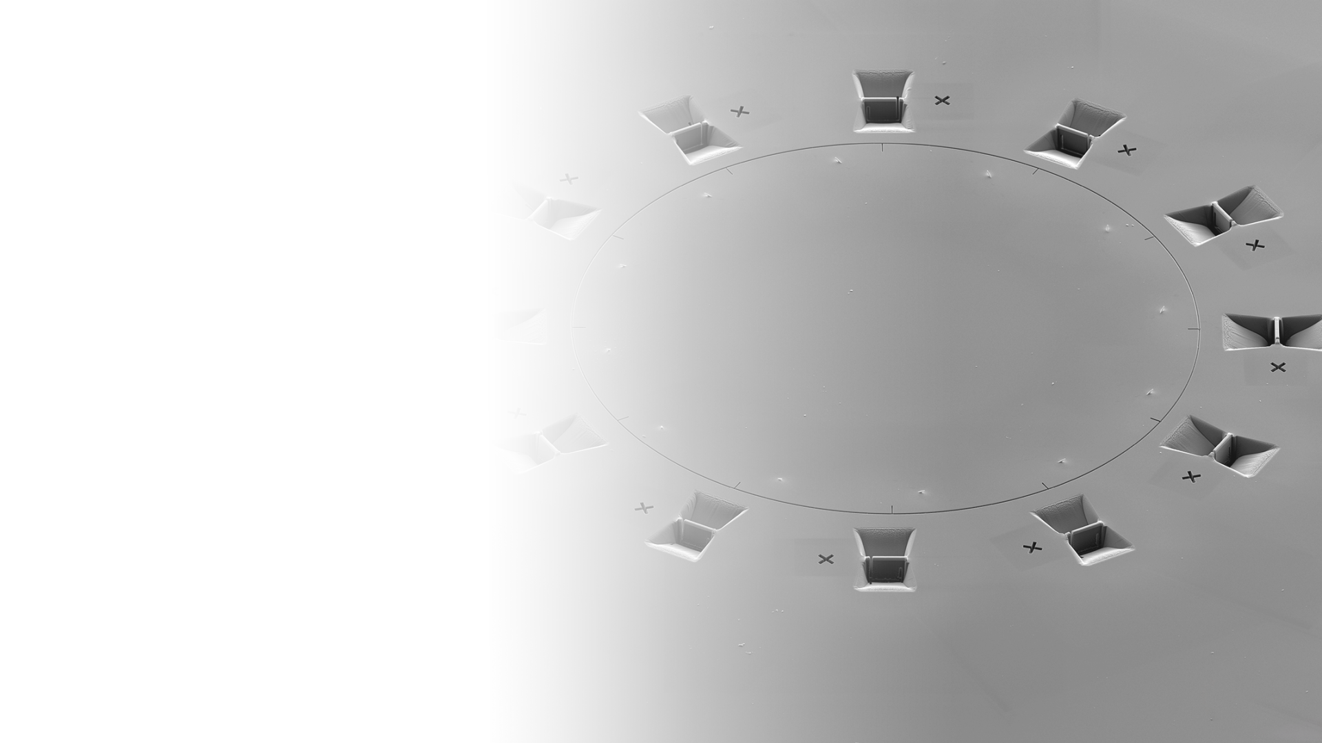
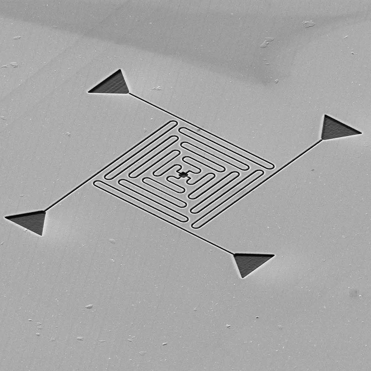
We are dealing with micro- and nanostructures for optical sensing [in our daily work]. Consequently, it is important to characterize devices on a nanometer scale.
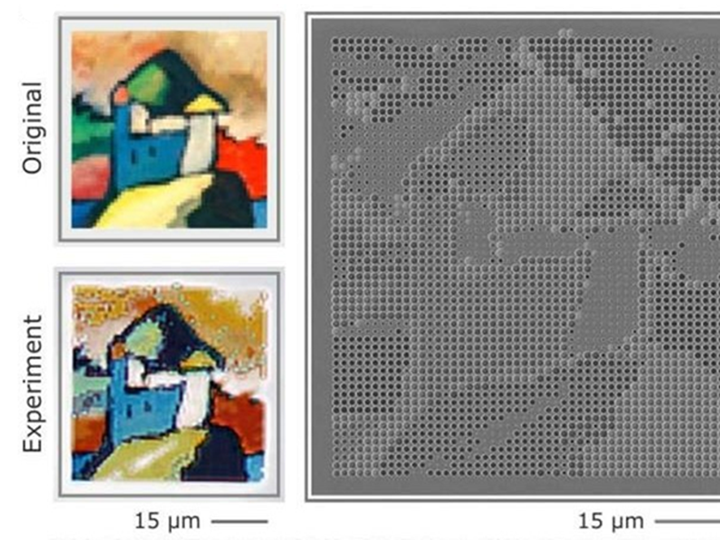
Learn How Dr. Mario Hentschel Addresses This Challenge With an Art Project
Third-party Content Blocked
The video player is blocked due to your cookie preferences. To change the settings and play the video, please click the button below and consent to use of "Functional" tracking technologies.
Discover a Slightly Different Nanomaterial Research Story
Not only in this Art Project with the Kandinsky from Stuttgarter Staatsgallery, Dr. Mario Hentschel made use of microscopy techniques that enable you to precicely image material at the nanoscale.
Review Advanced Material Characterization Technologies on the Market
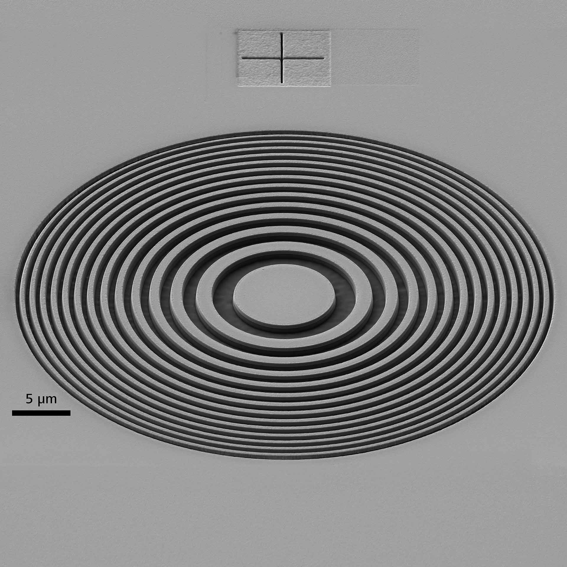
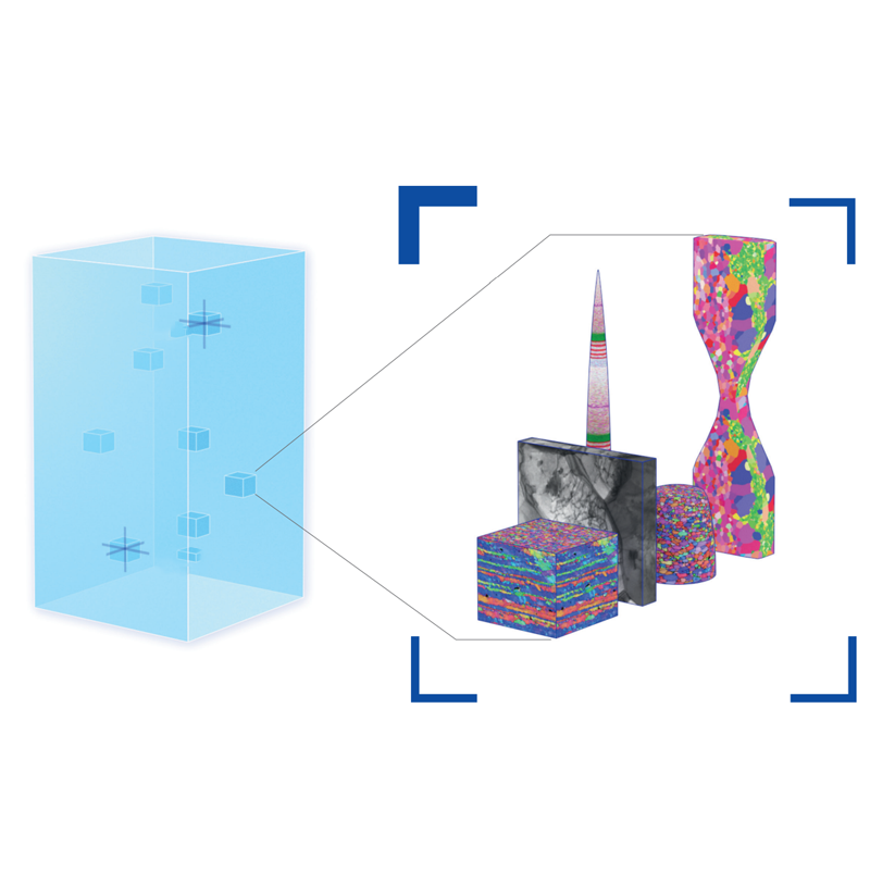
It’s vital that scientists select the most appropriate instrument for their needs - to ensure they can precisely and cost-effectively characterize samples. The instrument selection process often involves choosing an instrument that offers the sensitivity and resolution they require for sample analysis. Plus, the instrument must be easy-to-operate and maintain, with minimal downtime. instance, material scientists need to be able to explore material in as much detail as possible, locate and investigate regions of interest within a large sample, and effectively characterize large three-dimensional volumes
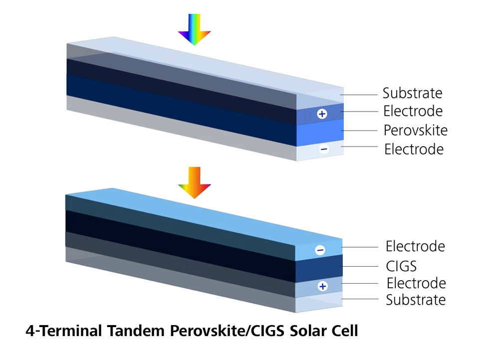
Microscopy is necessary for us to evaluate our layered systems [for solar cells].
Third-party Content Blocked
The video player is blocked due to your cookie preferences. To change the settings and play the video, please click the button below and consent to use of "Functional" tracking technologies.
Precisely Evaluate Your Layers at Nanoscale Level
"While the optical and electrical measurements provide us with the most relevant information about the solar cell function, we require materials analysis to relate the results to the processing."
The objective of my group is to work on new, ambitious and interdisciplinary ideas to trigger improved failure resistant material designs for industrial applications. Correlative Microscopy and Artificial Intelligence-Based Approaches are developed and utilized for efficient analysis and to gain a full understanding of the underlying structure-property relationship.
Multimodal Microscopy
Paired with AI Boosting Material Performance
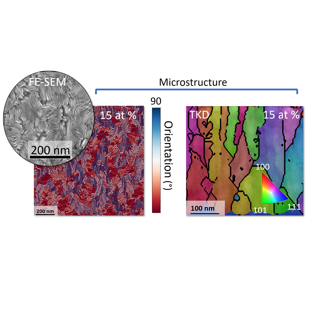
Roland Brunner's working group “Material and Damage Analytics” at the MCL is focussing on the development and utilization of advanced image-based methods (XCT, synchrotron nano-tomography, FIB-tomography, neutron-tomography, FESEM etc.) as well as on correlated imaging workflows. The group has a strong focus on materials for microelectronics and energy storage.
Although nanocrystalline metallic alloy thin films provide a variety of interesting properties especially for engineering applications there are some challenges which need to be solved. A big drawback concerns the generation of residual stresses evolving during the deposition process, limiting their performance.
Here, particularly the understanding of the stress evolution with respect to the occurrence of tensile and compressive stress within the thin film is of high importance for his group.
In general, the material microstructure impacts the material characteristics. Therefore, a profound knowledge of the underlying structure-property relationships is crucial for Roland Brunner and his group.
Discover How to Investigate the Microscopic World of Nanomaterials
Using Multimodal Microscopy
Find out more about optimizing sample preparation
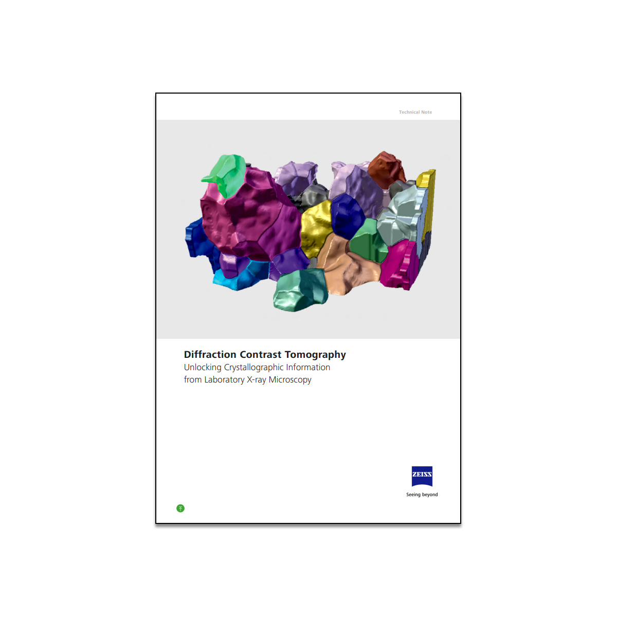
Learn how to obtain crystallographic information using diffraction contrast tomography
Explore the latest cutting-edge technologies designed to support both academic researchers and industries in materials science, including X-ray microscopy (XRM) tools